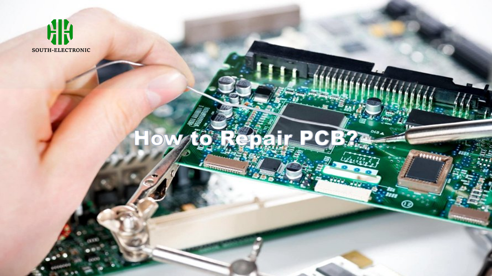
Having a broken PCB can ruin your day. Suddenly your project stops working. But don’t worry. It doesn’t mean the end. With the right tools, you can fix it yourself. Save money and time with simple pcb repair skills.
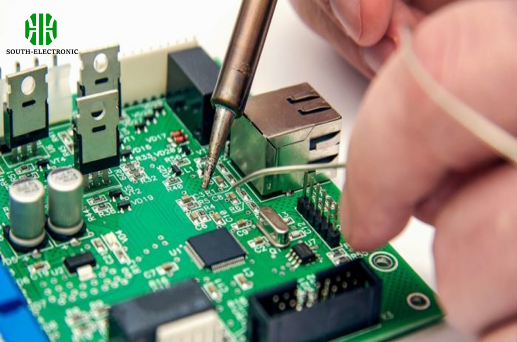
Identify the problem first – broken traces, missing pads, or damaged parts. Then use essential tools like a soldering iron and copper wires. Clean the area properly and reconnect using wire jumpers. This basic pcb repair process restores function without replacements.
Now you understand the basic steps for successful pcb board repair. But each problem needs different solutions. Let’s explore specific fixes every electronics hobbyist should know. I’ve used these methods for years in my projects.
How Can You Identify the Exact Failure Point on a PCB?
Finding the real trouble spot is hard. Without the right tools, you guess. Wasted time increases repair pcb frustration. Stop guessing and learn proven techniques.
Use visual checks first with good lighting. Then test with multimeter in continuity mode. This confirms broken connections. For hidden issues, apply power and watch for heat spots. These steps pinpoint any failure point every time.
Finding the failure spot has three critical parts. Each builds your PCB repair skills.
Step 1: Visual Inspection Methods
Look close without power first. I always start here after cleaning the PCB.
| Defect Type | Visible Signs |
|---|---|
| Burnt traces | Discoloration or charred lines |
| Lifted pads | Copper rings detached from board |
| Cracked solder | Fine lines around component feet |
| Broken traces | Physical gaps in copper lines |
Use a strong magnifier. Trace each path carefully. Burnt traces show dark marks. Lifted pads look uneven.
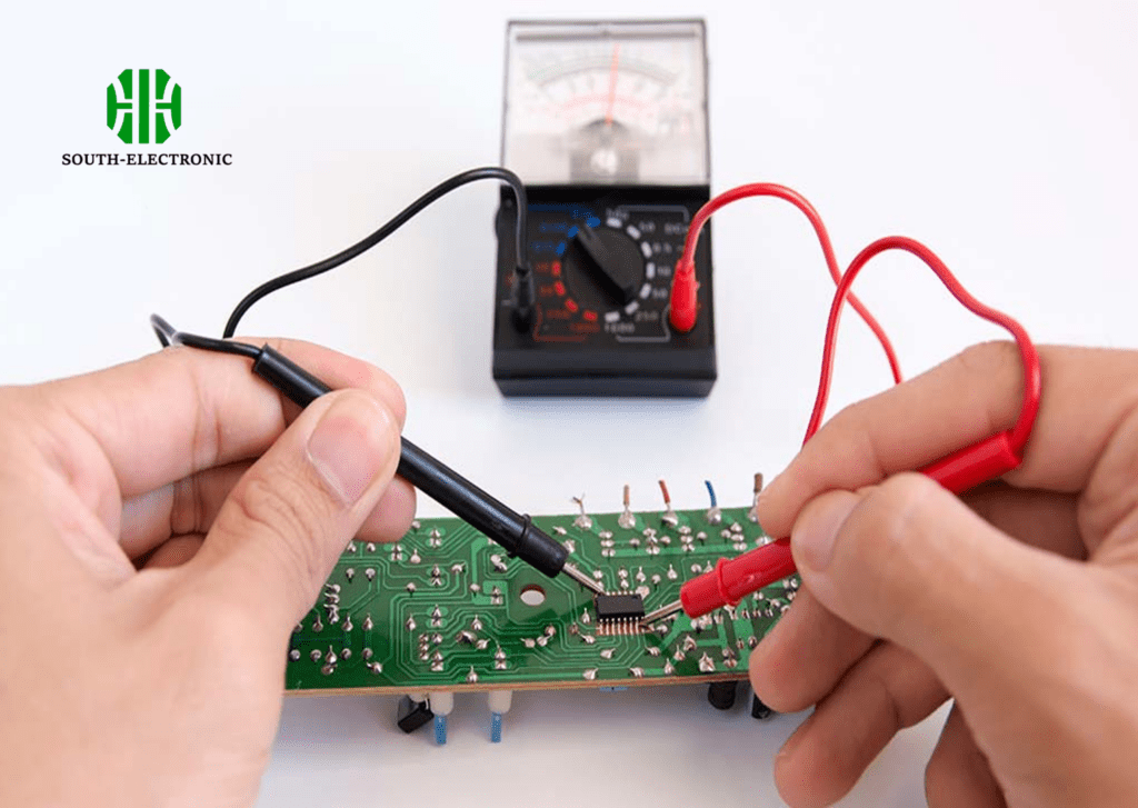
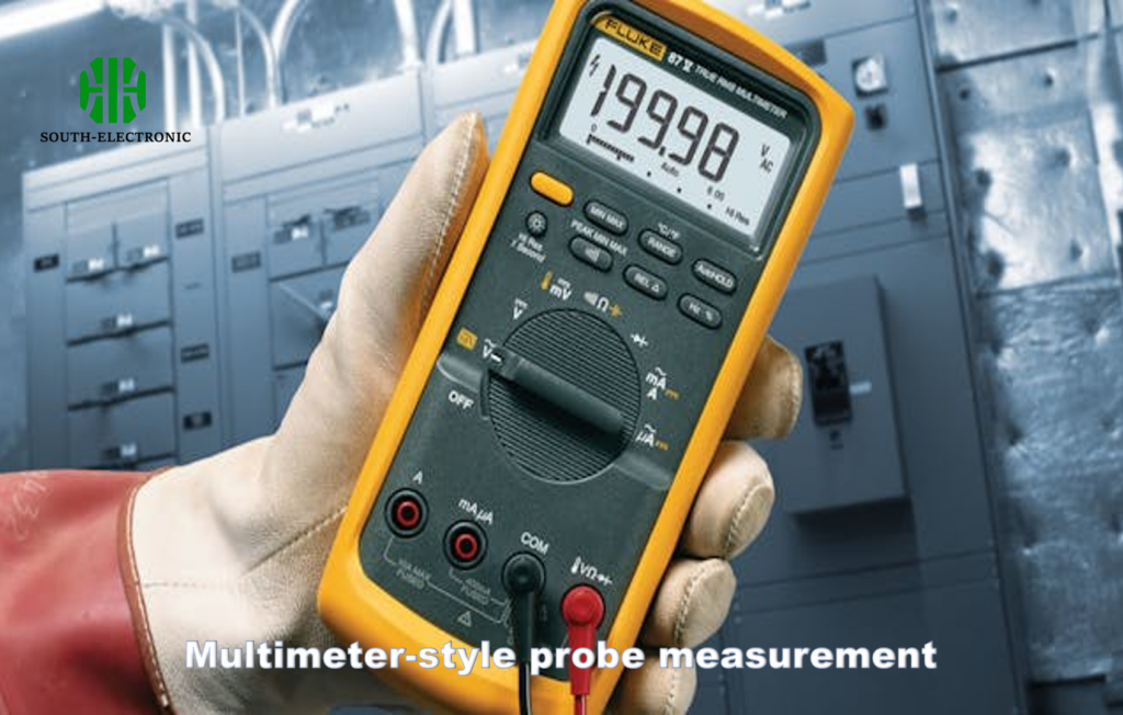
Step 2: Testing With Tools
If nothing shows, use your multimeter. Set to continuity mode like I do daily. Touch probe to trace start and end. No beep means break between points. Test components like capacitors for resistance problems. This tool handles most pcb circuit board repair needs.
Step 3: Advanced Detection
When basic methods don’t work try powering the board. Check for hot spots with temperature probes. Or apply pcb circuit trace repair kits conductive paint. Watch where electricity stops. Always isolate power sections first.
Start simple then advance up. Label suspect areas with tape. Documenting helps track progress.
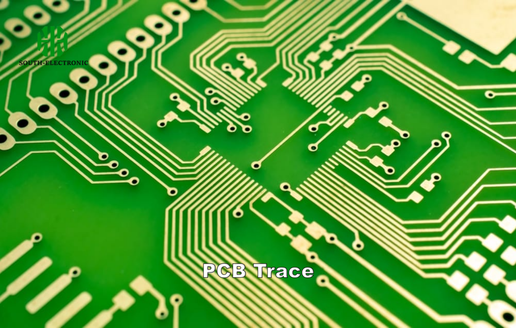
How to Repair PCB Trace?
Broken traces halt current flow. Without connection, your circuit fails. It feels impossible to fix tiny copper lines. But pcb trace repair is easier than you think.
Clean the damaged trace area thoroughly. Place wire jumpers across broken sections. Solder carefully to reconnect paths. This pcb circuit repair method revives non-working boards.
Fixing broken traces needs specific approaches. I learned these repairing hundreds of boards.
Repair Materials Comparison
Different gaps require different solutions.
| Material | Best For | Durability |
|---|---|---|
| Copper wire | Long trace breaks | Very strong |
| Conductive paint | Small gaps | Moderate |
| Solder bridges | Minor interruptions | Low |
I prefer copper wire for reliability. Automotive wires work great for pcb board repair kit use.
Step-by-Step Repair Process
- Scratch away solder mask from trace ends
- Cut thin insulated wire to needed length
- Strip wire ends clean using flush cutters
- Solder one end firmly to cleaned trace area
- Test alignment before attaching second end
- Apply flux and solder the other connection
After fixing burnt pcb trace, add epoxy coating. This protects against future damage. Let it cure overnight before testing.
Avoid overheating during repair. Too much heat destroys adjacent traces. Work in bright light so you see details.
How to Repair Lifted Pads on PCB?
Lifted copper pads make soldering impossible. Component legs hang loose without anchor points. It seems like the board is junk now. But good pad repairs save expensive circuits.
Clean exposed traces near the pad area. Attach thin wires to alternative points. Solder components through these connections instead. This repair lifted pad without soldering directly to damaged spot.
Lifted pads happen easily during rework. But repairs work if you know how.
Pad Repair Approach Matrix
Different pad types need different techniques.
| Pad Type | Recommended Repair Method | Stability |
|---|---|---|
| Small pads | Connect to nearby test point | Adequate |
| Anchored pads | Reinforce trace with epoxy | Good |
| Ground plane pads | Drill small hole and wire through | Excellent |
Ground plane repairs last longest in my experience. Use thin Teflon wires for flexibility.
Step-by-Step Solutions
First clean surrounding areas thoroughly. Then:
- Trace connected pathways under magnifier
- For exposed traces: solder jumper wire to undamaged segment
- Component legs connect to jumper’s free end
- Secure connections with tiny dot of epoxy
- For no exposed traces: create new anchor point
- Drill micro hole to opposite board side
- Thread component leg through entire hole
- Solder both sides securely
Prevent future lifting by heating slowly. Add adhesive during original assembly. Good pcb pad repair kit makes jobs easier.
When Should You Replace Components vs Resolder Them?
Damaged parts can mislead you. Resolding seems faster than replacement. But it wastes time if part is bad. Knowing when to swap saves hours.
Resolder first when solder joints look cracked or loose. Replace components if physical damage appears. Burnt, bulging, or leaking parts always need replacement. Testing prevents unnecessary swaps.
Component replacement decisions affect repair longevity. Use these guidelines I follow.
Repair Decision Factors
Three key factors guide best approach.
| Factor | Replace Component | Resolder Joint |
|---|---|---|
| Component age | Over 5 years | Under 2 years |
| Physical state | Burnt or swollen | Intact appearance |
| Test results | Fails measurement | Passes diagnostics |
If unsure, test components first. Multimeter checks prevent mistakes.
Step-By-Step Component Management
Here’s my process for cost-effective repairs:
- Clean joint with alcohol and inspect closely
- Apply fresh flux and hot air to existing joint
- If problem persists, test component separately
- Resistor failures always need replacement
- Integrated circuits often require swapping
- For multilayer boards, consider cost to repair 4 layer pcb factors
- Replace only clearly damaged parts
- Solder new identical components carefully
Document all replacements. Track inventory for future repair pcb needs.
Conclusion
PCB repair starts with problem diagnosis. Fix traces and pads using simple methods. Replace only damaged parts carefully. These skills save boards from becoming e-waste.