
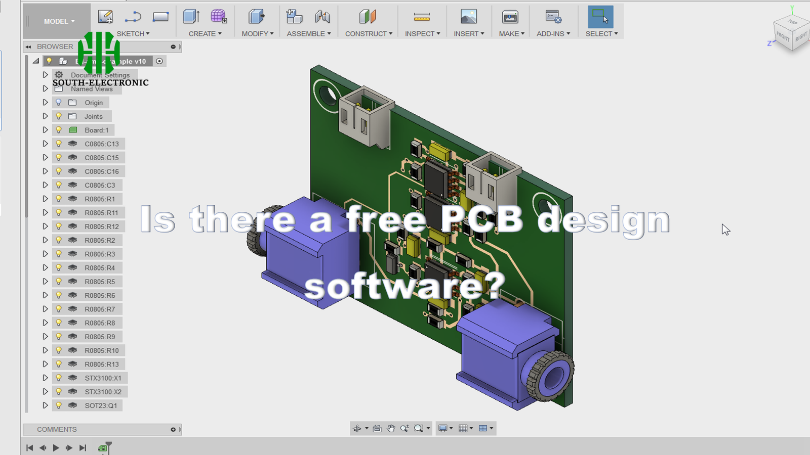
Designing PCB boards often feels expensive. New users struggle with costly tools. Your project budget might get drained quickly. Don’t worry about wasting money anymore. Free solutions do exist for you.
Yes, multiple free pcb layout software options deliver professional features. Tools like KiCad and EasyEDA offer full schematic capture and PCB design capabilities without hidden fees. These solutions let you create complex boards at zero cost.

Let’s explore these game-changing free pcb design solutions in detail. I’ll guide you through each option’s strengths for different needs.
Are there any truly free PCB design tools?
Cost traps in PCB software worry many designers. Some "free" tools restrict export features. Others block critical functions behind paywalls. You deserve genuinely open access.
Truly free choices exist with unlimited capabilities. KiCad and LibrePCB offer complete pcb board layout software without paid tiers. Both support schematic-to-production workflows with no forced subscriptions.
Key Features Comparison
| Feature | KiCad | LibrePCB | EAGLE Free |
|---|---|---|---|
| Board Layers | Unlimited | Unlimited | 2 Signal Layers |
| Schematic Sheets | No Limit | No Limit | 1 Sheet |
| Board Size | Any Dimension | Any Dimension | 80cm² Maximum |
| Part Libraries | Community-Driven | Built-in Manager | Limited Selection |
| File Export | All Formats | All Formats | Restricted Formats |
KiCad stands out for advanced users needing complex designs. I recently designed a 4-layer IoT board using only its tools. The community constantly adds new part libraries automatically. LibrePCB simplifies project organization with unique "library concepts". Both allow commercial use with no licensing worries. EAGLE’s free version works for simple single-sided boards but shows limitations quickly. Avoid unexpected costs by choosing open-source options first.
What’s the Best PCB Layout Software for First-Time Learners?
Starting PCB design feels overwhelming. Complex interfaces create frustration. Beginners waste hours searching basic functions. You need clear pathways to success.
EasyEDA wins for new users with gentle learning curves. Its browser-based pcb design online platform includes guided tutorials and ready-to-use templates. CircuitMaker’s visual feedback helps beginners spot mistakes quickly.
Learning Experience Compared
| Aspect | EasyEDA | CircuitMaker | Fritzing |
|---|---|---|---|
| Interface Simplicity | Drag-and-Drop Simple | Visual Toolbars | Breadboard View |
| Built-in Tutorials | Interactive Step Guides | Video Demonstrations | Limited Instructions |
| Component Library | Integrated Online Parts | Managed Community | Basic Starter Set |
| Error Checking | Real-Time Highlighting | Design Rule Checks | Minimal Validation |
EasyEDA helps most when starting your first schematic. Its online circuit simulator immediately shows if connections work right. Circuit Maker organizes projects visually which eases navigation confusion. Fritzing shows practical breadboard layouts but lacks professional output quality. For learning free pcb layout software, start browser-based for instant access anywhere.
Is there any mobile phone software that can be used for PCB layout?
Mobile viewing of PCB designs brings convenience. Engineers often need quick checks during travel. Factory visits require immediate design access. Can phones handle actual PCB work?
Limited mobile solutions exist mainly for viewing. Autodesk Viewer allows EAGLE file checks. KiCad cannot run natively on phones due to computing needs. Touch interfaces complicate precise placement required for pcb layout softwares.

Mobile Capability Overview
| Function | Autodesk Viewer | EasyEDA App | Web Browser Access |
|---|---|---|---|
| Design Viewing | Full Schematic | Basic Layout | Limited Pan/Zoom |
| Real Edit Capable | Measurements Only | Component Placing | Impossible |
| Library Management | No Component Access | Part Browser | Not Available |
| File Compatibility | EAGLE Files | EasyEDA Projects | PDF/Gerber Viewing |
True PCB layout demands keyboard and mouse precision. I once tried adjusting traces on a tablet during commute and produced multiple errors. While EasyEDA app allows emergency placements, always finalize designs on desktop. Mobile remains best for quick checks of existing free pcb design files.
Conclusion
Great free pcb layout software exists for all levels. KiCad and EasyEDA offer professional options without cost barriers. Start projects confidently with these accessible tools.

