

Have you ever wondered how your smartphone’s brain is built? I felt overwhelmed learning how tiny green boards power electronics. Understanding the PCB manufacturing process solved my confusion and empowered my projects.
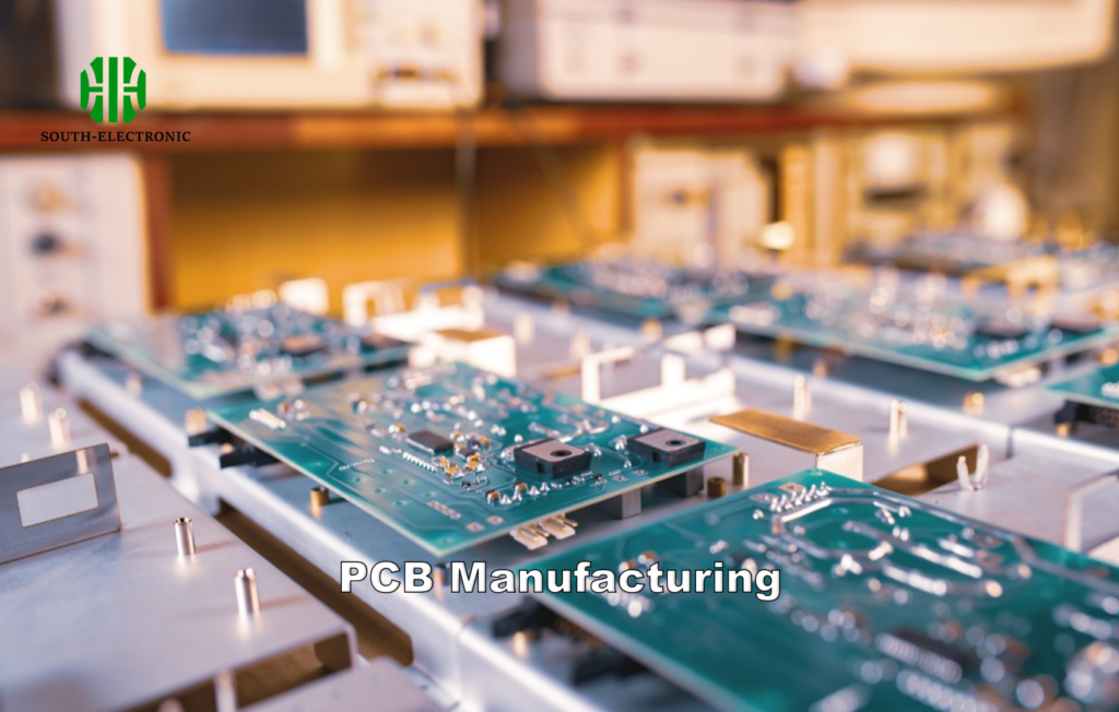
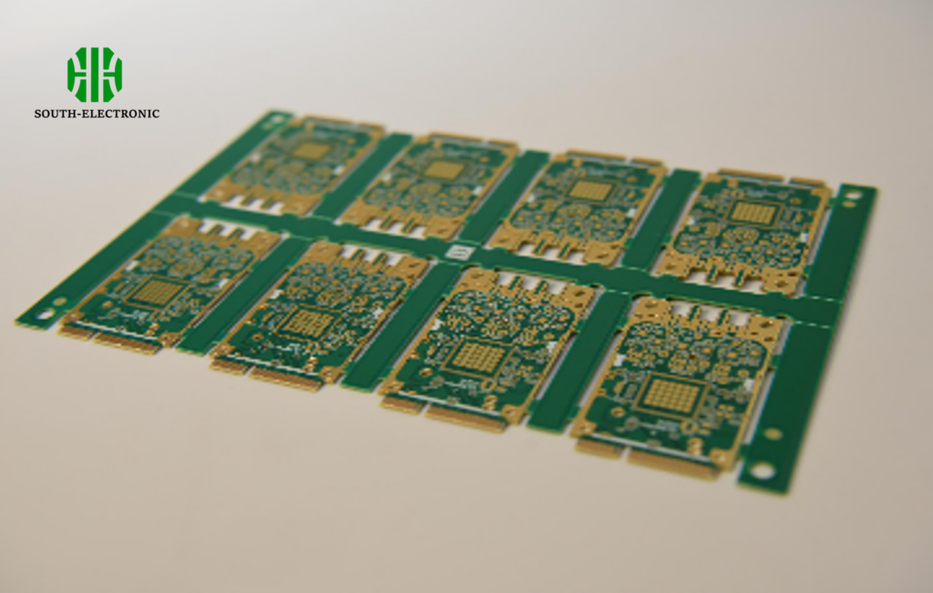
PCB manufacturing transforms designs into functional boards through 12 precise stages. Materials are layered, etched, drilled, and tested to create reliable circuits. This process applies to all boards, whether rigid or flexible.
Knowing these steps helps you collaborate effectively with printed circuit board manufacturers. Let’s explore each critical phase and specialized manufacturing choices.
What Are the 12 Critical Steps in PCB Manufacturing?
Staring at my first PCB blueprint, I panicked about potential errors. Skipping any manufacturing step risks dead boards. Precise execution matters for functional electronics.
The core stages are design review, imaging, etching, AOI inspection, lamination, drilling, plating, outer imaging, etching, solder mask, silkscreen, surface finish, testing, and routing. Each ensures electrical integrity and durability.
Breaking Down the Process
The printed circuit board manufacturing process demands precision:
Design Preparation
- Engineers verify design files (Gerber)
- Material selection (FR-4, aluminum, or flex substrates)
| Stage | Purpose | Common Issues |
|---|---|---|
| Inner Layer Imaging | Transfers circuit pattern | Over/under-exposure |
| Etching | Removes unwanted copper | Over-etching |
| AOI Inspection | Detects inner layer defects | Micro-cracks |
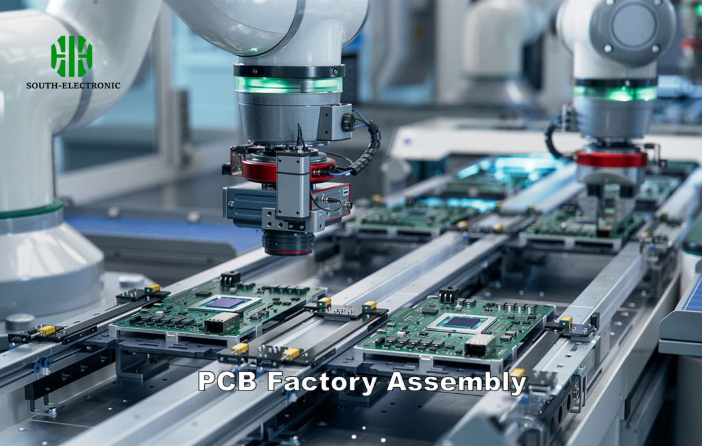
Board Assembly
After lamination, mechanical drills create holes for components. Electroplating deposits copper to connect layers. Final etching defines outer circuits.
Quality Control
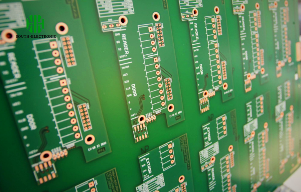
Solder mask application prevents shorts. Silkscreen adds labels. Flying probe tests validate connections before V-scoring separates boards. Rigorous testing catches 99.7% of faults.
How Does Flexible PCB Manufacturing Differ From Rigid Boards?
My smartwatch repair revealed flimsy circuits unlike rigid phone boards. Flexible printed circuit manufacturers use unique methods for bendable electronics.
Flexible PCBs use polyimide instead of fiberglass, require laser drilling, and undergo specialized lamination. They skip mechanical routing – instead employing laser cutting or chemical etching for precision shaping.

Key Differences Explained
Flexible printed circuit board manufacturers prioritize adaptability:
Material Differences
- Flex: Polyimide films (heat-resistant, bendable)
- Rigid: FR-4 fiberglass (rigid, cost-effective)
| Process Step | Flexible PCB | Rigid PCB |
|---|---|---|
| Substrate | Polyimide/Kapton | FR-4 |
| Conductive Layers | Rolled annealed copper | Electro-deposited copper |
| Adhesives | Acrylic based | Epoxy based |
Specialized Processing
Lamination uses lower pressures for flex boards. Laser drilling creates microscopic vias. Etching requires finer tolerances. Final testing includes dynamic bending cycles. Most flexible printed circuit manufacturers charge 30-50% more due to these complexities.
USA vs China vs India: Which Region Fits Your PCB Manufacturing Needs?
Choosing between regions felt like gambling with my startup budget. Each offers distinct advantages for printed circuit board manufacturing.
China prioritizes scale and cost efficiency, USA excels in prototyping and IP security, India balances moderate pricing with growing quality. Your choice depends on volume, complexity, and compliance needs.
Regional Capability Analysis
Critical factors when selecting printed circuit board manufacturers:
Prototyping Needs
- USA: Best for <100 boards (2-3 day turnaround)
- India: Mid-volume prototypes (5-7 days)
- China: Economical only for 500+ units
| Regulatory Compliance | Region | Lead Time | Cost Index | Specializations |
|---|---|---|---|---|
| USA | Short | High | Aerospace/medical | |
| China | Long | Low | Consumer electronics | |
| India | Medium | Medium | Industrial automation |
Scalability Concerns
China dominates mass production through automation – ideal for simple boards. American printed circuit board manufacturers in usa offer tighter tolerances for complex designs. India’s emerging infrastructure provides competitive pricing for mid-volume orders.
5 Must-Ask Questions When Auditing PCB Manufacturers
After receiving warped boards from a vendor, I created this audit checklist. These questions uncover true manufacturing capabilities.
Ask: 1) Certifications held (ISO/UL) 2) Maximum layer capacity 3) DFM feedback process 4) Testing equipment used 5) Percentage of rework orders. Answers reveal true expertise.
Critical Audit Framework
When visiting printed circuit board assembly manufacturer facilities:
Technical Capability Check
- Verify equipment: Flying probe testers? Laser drills?
- Request throughput data and defect rates
| Question | Red Flag | Green Flag |
|---|---|---|
| "Can you handle HDI designs?" | "We outsource microvias" | In-house laser drilling |
| "Show IPC Class 2 examples" | No documentation | Production samples |
Compliance Verification
Confirm RoHS/REACH certificates. Ask about conflict mineral policies. Prototype printed circuit board manufacturers often skip these checks – require evidence.
Operational Transparency
Good sign: They showcase AOI rejection logs. Bad sign: Hidden rework stations. Reputable printed circuit board manufacturers uk provide real-time production tracking.
Conclusion
Understanding the PCB manufacturing process helps you select the right partner and design reliable boards. Always verify manufacturer capabilities against your project requirements.

