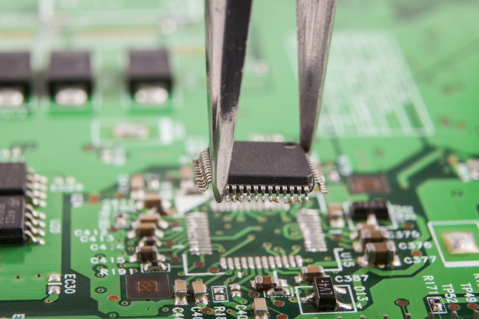
Feeling limited by single-layer boards? Need more power, more features, in less space? Multilayer PCBs are the answer you've been searching for.
Multilayer PCBs stack multiple circuit layers, separated by insulation, into a single unit. This design allows for incredibly compact and powerful electronic devices[^1], making them essential for modern technology where space is at a premium.
I remember struggling with complex circuits, trying to fit everything on a single board. It was frustrating, and I knew there had to be a better way. That's when I discovered multilayer PCBs. Now, I can achieve densities and performances I once thought impossible. Let me show you how.
Why are multilayer PCBs so widely used?
Are your designs getting too crowded? Do you need more functionality in a smaller package? Multilayer PCBs solve these problems, becoming essential for today's compact electronics.
Multilayer PCBs are widely used because they offer unparalleled density and performance in a small footprint. They allow for complex interconnections and dedicated power planes, meeting the demands of modern, powerful, and miniaturized electronic devices.

In a world that demands more powerful and smaller devices, the simple truth is that single-layer boards just don't cut it anymore. Think about your smartphone—it's a marvel of engineering, packed with features. This wouldn't be possible without multilayer PCB technology. The ability to stack multiple layers of circuitry, isolated by dielectric materials, means designers can route signals in three dimensions, rather than just two. This dramatically increases routing density[^2] without increasing the overall size of the board. Dedicated power and ground planes can also be incorporated, which are crucial for signal integrity and reducing electromagnetic interference (EMI)[^3] in high-speed applications. As I see it, the trend towards miniaturization and increased functionality will only continue, making multilayer PCBs not just a choice, but a necessity for most advanced electronic products.
| Feature | Single-Layer PCB | Multilayer PCB |
|---|---|---|
| Space Efficiency | Low | High |
| Circuit Density | Low | Very High |
| Performance | Basic | Advanced, High-Speed |
| Cost | Lower initial | Higher initial |
| Complexity | Simple | Complex |
What are the benefits of multilayer PCBs?
Struggling to fit all your components? Want better performance from your circuits? Multilayer PCBs offer significant advantages, making them a game-changer for complex designs.
Multilayer PCBs provide compact size, higher component density, improved electrical performance due to shorter signal paths and dedicated planes, and enhanced durability. These benefits are critical for creating advanced, reliable electronic products.

From my experience, the benefits of multilayer PCBs extend far beyond simply fitting more components. One of the most impactful advantages is the compact size and weight. By stacking layers, you effectively "fold" the circuit, dramatically reducing the physical footprint. This is crucial for portable devices where every millimeter and gram counts. Another key benefit is higher component density. More routing paths mean you can place more components in a given area, leading to more powerful devices. Better electrical performance is also huge. Shorter signal paths reduce latency and improve signal integrity, especially at high frequencies. Dedicated ground and power planes act as shields, minimizing crosstalk and noise, which is vital for sensitive analog or high-speed digital circuits. Finally, the robust construction provides high quality and durability, making them suitable for demanding environments. I've seen firsthand how these boards improve reliability.
| Benefit | Description |
|---|---|
| Compact Size & Weight | Layers are stacked, reducing overall board size and weight, ideal for miniaturized devices. |
| Higher Component Density | More routing area allows for denser component placement, increasing functionality. |
| Improved Electrical Performance | Shorter signal paths, better EMI shielding, and dedicated power planes enhance signal integrity. |
| Enhanced Durability | Staggered layers and compact design provide greater structural stability and heat resistance. |
| Single-Point Connectivity | Centralized connections simplify assembly and improve reliability. |
What are the disadvantages of multilayer PCBs?
Considering multilayer PCBs, but worried about potential drawbacks? Every advanced technology has its challenges. Let's explore the cons.
Despite their benefits, multilayer PCBs come with higher manufacturing costs[^4], increased design complexity, and more challenging repair processes[^5] compared to single or double-sided boards. These factors require careful consideration during product development.
While I'm a big proponent of multilayer PCBs, it's important to have a balanced view. There are definite disadvantages to consider. The most obvious is higher cost. Manufacturing multilayer boards involves more steps, specialized equipment, and tighter tolerances, which directly translates to a higher price per board. This can be a significant barrier for low-cost products or startups with limited budgets. Secondly, increased design complexity is a real factor. Routing across multiple layers requires sophisticated CAD tools and experienced designers. Managing impedance, crosstalk, and thermal dissipation in a 3D structure is far more challenging than on a 2D plane. Finally, repair and rework are significantly harder. Once layers are laminated, accessing internal traces for repairs is nearly impossible. A tiny manufacturing defect in an inner layer often renders the entire board unusable, leading to higher scrap rates. I've learned that careful planning and simulation are critical to mitigate these risks.
| Disadvantage | Impact | Mitigation Strategy |
|---|---|---|
| Higher Manufacturing Cost | More materials, complex processes, and specialized equipment increase unit cost. | Optimize layer count, leverage volume production. |
| Increased Design Complexity | Requires advanced CAD tools and experienced designers for routing and signal integrity. | Use DFM (Design for Manufacturability) guidelines, simulation tools. |
| Difficult Repair/Rework | Internal layers are inaccessible, making repairs extremely challenging or impossible. | Rigorous testing at each stage, robust design, quality control. |
| Longer Lead Times | Complex fabrication processes can extend manufacturing schedules. | Plan ahead, work with reliable manufacturers. |
Is South-Electronic's multilayer PCB high precision and professional?
Looking for reliable, high-quality multilayer PCBs? Wondering if South-Electronic meets the demanding standards of modern electronics? Let's assess their capabilities.
South-Electronic's multilayer PCBs are known for their high precision and professional manufacturing, enabling complex designs for demanding applications. They utilize advanced processes and strict quality control to deliver boards that meet industry-leading standards for performance and reliability.

From what I've gathered, South-Electronic has positioned itself as a reputable manufacturer in the multilayer PCB space, particularly for applications requiring high precision. When I evaluate a supplier, I look for a few key things: Advanced Manufacturing Capabilities. Do they have state-of-the-art equipment for lamination, drilling, and plating? For multilayer boards, this is non-negotiable. Precision alignment of layers is paramount for signal integrity and avoiding short circuits. I also consider their Quality Control Processes. Are there stringent checks at every stage, from raw material inspection to final electrical testing? This is especially critical for multilayer boards where defects in inner layers are difficult to detect until late in the process. Furthermore, their focus on high-density interconnect (HDI) technology[^6] suggests a commitment to supporting the industry's drive towards miniaturization and increased functionality. This often includes features like micro-vias[^7] and fine line spacing[^8], which are hallmarks of professional, high-precision manufacturing.
| Aspect | South-Electronic's Approach |
|---|---|
| Precision Manufacturing | Utilizes advanced lamination, drilling, and etching processes for tight tolerances and accurate layer alignment. |
| Quality Control | Implements rigorous inspection at each production phase, including AOI (Automated Optical Inspection) and electrical testing. |
| Material Selection | Offers a range of high-performance dielectric materials suitable for various applications and thermal demands. |
| Technical Expertise | Provides engineering support for complex designs, including impedance control and stack-up optimization. |
| Certifications | Often holds industry certifications (e.g., ISO, UL) demonstrating adherence to global quality and safety standards. |
Conclusion
Multilayer PCBs are vital for modern electronics, offering compact, high-performance solutions. Weighing benefits against costs is key, and choosing a precision manufacturer like South-Electronic ensures quality.
[^1]: Discover how multilayer PCBs enable the creation of advanced electronic devices. [^2]: Explore how increased routing density in multilayer PCBs leads to better performance. [^3]: Learn about the techniques multilayer PCBs use to minimize EMI in electronic devices. [^4]: Understand the factors contributing to the higher costs of multilayer PCB production. [^5]: Discover the difficulties in repairing multilayer PCBs and how they impact product lifecycle. [^6]: Discover how HDI technology contributes to the miniaturization of electronic devices. [^7]: Learn about micro-vias and their role in enhancing multilayer PCB functionality. [^8]: Explore the importance of fine line spacing for achieving high-density designs.


