
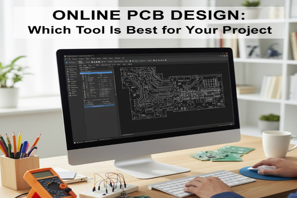
Struggling to find the right PCB design software? Mistakes cost money and time. Choose wisely based on project needs.
The best tool balances functionality and accessibility. I recommend EasyEDA for most projects - it's free, web-based, and covers schematic to layout. Alternatives exist for specific needs.
Understanding key differences helps avoid frustration. Let's explore crucial selection factors.
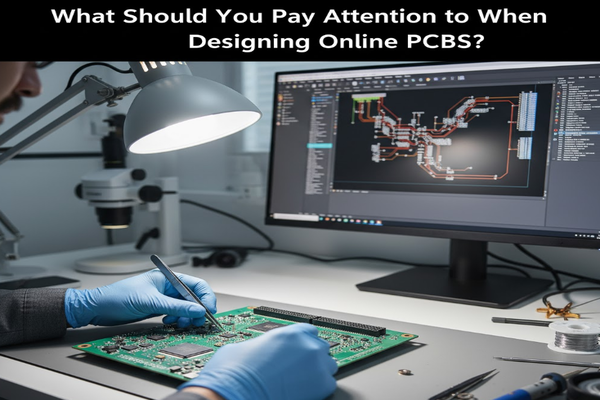
What Should You Pay Attention to When Designing Online PCBs?
Overlooked design flaws ruin projects? Avoid frustration by focusing on core elements.
Critical areas include component availability[^1], trace routing[^2], and design rules[^3]. Verify manufacturing compatibility early. I once saved weeks by checking part availability first.
Successful designs require methodical attention.
Key Design Fundamentals
Three pillars determine success: component planning, routing precision, and rule validation. Neglecting any causes manufacturing delays.
Component Selection Mistakes
Avoid rare or obsolete parts. Cross-check distributors before finalizing. My solar project stalled due to an unavailable microcontroller. Create backup options.
Routing and Signal Quality
Prioritize trace clearances and angles. Straight 45-degree traces prevent signal issues. Minimum spacing depends on voltage requirements.
Design Rule Validation
Every manufacturer has specifications. Define these early:
| Key Parameter | Standard Value | Impact of Deviation |
|---|---|---|
| Trace Width | 0.2mm | Overheating/breakage |
| Hole-to-Trace Space | 0.15mm | Manufacturing defects |
| Silkscreen Clearance | 0.1mm | Assembly difficulties |
Run automated DRC checks[^4] at every stage. Adjust rules after consulting your manufacturer.
Are Online PCB Design Software Programs Really Free and Easy to Use? Which One Do You Prefer?
"Free" claims misleading? Some hide costs behind steep learning curves.
Most offer free tiers with limitations. EasyEDA remains truly free for core features. I prefer its balance. Paid tools like Altium 365 excel for complex team projects.

Tool selection depends on need specifics.
Cost Reality Check
"Free" often means limited exports or private projects. Paid tiers add collaboration and advanced features. EasyEDA breaks this pattern with unlimited capabilities.
Usability Comparison
I've tested all major platforms:
- EasyEDA[^5]: Intuitive drag-and-drop interface (3 days to master)
- KiCad[^6]: Steeper curve but powerful (2 weeks proficiency)
- Altium 365[^7]: Professional features (requires training)
Performance Analysis
Evaluate based on workload:
| Tool | Hobby Projects | Professional Use | Team Collaboration |
|---|---|---|---|
| EasyEDA | Excellent | Good | Limited |
| KiCad | Good | Excellent | Difficult |
| Altium 365 | Overkill | Outstanding | Outstanding |
Choose KiCad for open-source projects. Use EasyEDA for quick turnarounds.
Will PCB Manufacturers Provide Online PCB Designs for You?
Need design help but lack skills? Manufacturers offer support - for a price.
Most manufacturers provide design services at extra cost. Fees vary by complexity. You sacrifice creative control despite faster turnaround.

Weigh benefits against constraints.
Service Cost Structure
Basic layout adjustments cost $100-300. Full custom designs[^8] range from $500-$5000+. Complex boards require deeper investment.
Critical Limitations
Manufacturers optimize for their processes, not innovation. My RF design lost custom features through their "optimization." You'll compromise control.
Decision Framework
Answer these questions:
- How complex is your solution?
- Do you have specific component requirements?
- Can you afford multiple iterations?
Consider manufacturer help only when:
- Facing tight deadlines
- Building exceptionally dense boards
- Using exotic materials Compare five service providers minimum before committing.
Conclusion
Match tools to project needs: EasyEDA for simplicity, KiCad for customization. Manufacturers help with complex or rushed designs.
[^1]: Learn why ensuring component availability is crucial for successful PCB projects. [^2]: Understand the significance of trace routing and how it affects your PCB's performance. [^3]: Discover the key design rules that can prevent manufacturing defects in your PCB. [^4]: Find out how automated DRC checks can enhance the reliability of your PCB designs. [^5]: Explore how EasyEDA's features can streamline your PCB design process and save you time. [^6]: Explore KiCad's powerful features and why it's a great choice for open-source projects. [^7]: Learn about Altium 365's advanced features that cater to complex team projects. [^8]: Explore the complexities and considerations involved in creating custom PCB designs.

