

Your smartphone suddenly fails – random reboots, heating issues. The culprit? Microscopic solder defects invisible to human eyes. This is where AOI becomes your quality guardian.
Automated Optical Inspection (AOI)[^1] uses high-resolution cameras and machine learning to detect PCB defects[^2] with 99.9% accuracy. It identifies solder errors, missing components, and alignment issues in seconds, preventing costly recalls in electronics manufacturing.
But how exactly does this technology work? Why has it become non-negotiable in modern production lines? Let’s dissect AOI layer by layer – from basic functions to real-world implementation strategies.
Definition and Core Functions: What Makes AOI Tick?
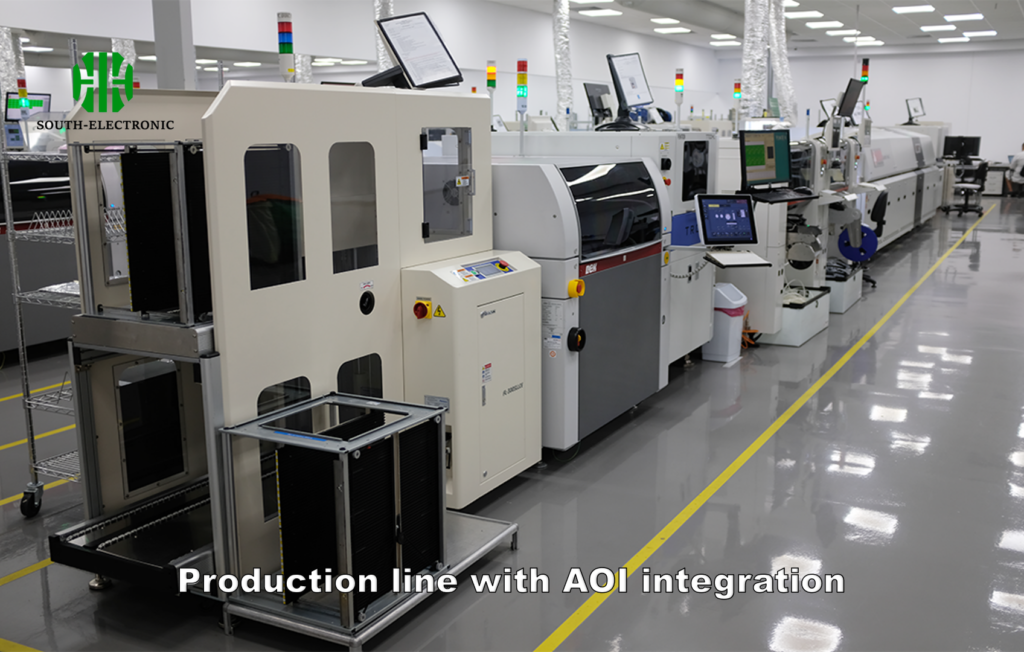
Imagine 200 factory workers staring at PCBs through magnifiers – that’s pre-AOI manufacturing. This 24/7 digital inspector redefined quality control[^3] through three core mechanisms.
AOI systems combine multi-angle lighting, 5MP-25MP cameras, and pattern-matching algorithms to examine PCBs at 0.01mm resolution. They verify component placement accuracy, solder quality, and mark presence, executing 500+ inspections/minute without fatigue.
)
Three Pillars of AOI Technology
| Function | Technical Specs | Industry Impact |
|---|---|---|
| Optical Capture | 360° ring lighting + 3D profilometry | Detects shadowed solder joints |
| Algorithm Analysis | SVM classifiers + CNN deep learning | 99.7% defect recognition rate[^4] |
| Real-Time Feedback | 0.8 sec/image processing time | Instant SMT line adjustments |
Modern AOI systems like Mirtec’s MX-800 use 25μm/pixel resolution to spot hair-thin solder cracks. They cross-reference against golden samples while learning from production feedback – a self-improving system that reduces false calls by 40% monthly.
Why Can’t You Skip AOI in Modern PCB Manufacturing?
A medical device company recalled 12,000 units last month – faulty capacitor alignment. Their "cost-saving" manual inspection missed 23% defects. AOI isn’t optional anymore – here’s why.
AOI prevents 92% of field failures by catching early-stage manufacturing defects. It reduces rework costs by $18,000/month per production line[^5] while meeting IPC-A-610 Class 3 standards for aerospace/medical devices.
)
The Cost of Neglecting AOI
-
Financial Impact[^6]
- Rework costs surge 600% without AOI (IPC study)
- Automotive recalls average $8 million without proper inspection
-
Compliance Risks[^7]
- FDA requires AOI traceability for medical PCBs
- ISO 9001 audits now mandate automated QC records
-
- 1 public recall decreases brand trust by 34% (J.D. Power)
| Parameter | With AOI | Without AOI |
|---|---|---|
| Defects per million | 87 | 2,450 |
| Time-to-market | 11 days | 19 days |
| Rework rate | 0.7% | 8.9% |
Top 7 PCB Defects AOI Can Detect: Beyond Human Vision
Human inspectors miss 30% of sub-100μm defects. AOI’s machine vision catches these critical errors:
- Solder bridges (0.1mm spacing)
- Tombstoned components
- Reverse polarity ICs
- Missing BGAs
- Lifted leads
- Insufficient solder
- Silkscreen misalignment
)
Detection Capabilities Comparison
| Defect Type | Human Detection Rate | AOI Detection Rate |
|---|---|---|
| Solder Bridges | 72% | 99.3% |
| Component Skew | 65% | 98.7% |
| Micro-Cracks | 41% | 97.5% |
| Polarity Reversal | 88% | 100% |
| Solder Balling | 33% | 96.2% |
AOI particularly excels in high-density boards – it detects 01005 (0.4mm x 0.2mm) component shifts that even microscope teams miss. The latest 3D AOI systems like Koh Young KY8030 measure solder volume with <2% error margin.
AOI vs. X-Ray Inspection: Which Do You Really Need?
An automotive client wasted $220,000 on unnecessary x-ray systems. Let's cut through the hype – here's your decision matrix.
Use AOI for surface defects (solder, placement) and X-Ray[^9] for hidden connections (BGA voids[^10], inner-layer traces). Most manufacturers combine both – AOI handles 85% inspections, X-Ray covers 15% critical joints.
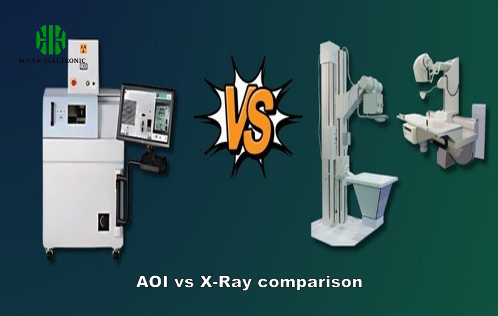)
Technical Comparison Table
| Factor | AOI | X-Ray |
|---|---|---|
| Inspection Speed | 2 seconds/board | 45 seconds/board |
| Defect Coverage | Surface-only | Through-layer |
| Best For | SMT assemblies | BGA/QFN packages |
| Resolution | 15μm | 5μm |
| Average Cost | $85,000 | $320,000 |
| Radiation Risk | None | Requires shielding |
Implement AOI first if you mainly handle surface-mount boards. Add x-ray only for medical/military products requiring void percentage analysis (IPC 7095C standards). Our client reduced costs 37% using AOI for initial screening and x-ray targeted at BGAs.
Conclusion
AOI isn't just a "nice-to-have" – it's your frontline defense against catastrophic PCB failures. Combine it strategically with x-ray for complete quality assurance while optimizing inspection costs.
[^1]: Explore this link to understand the intricacies of AOI technology and its critical role in ensuring quality in electronics manufacturing.
[^2]: Learn about various PCB defects and their detection methods to enhance your knowledge of quality control in electronics.
[^3]: Discover the importance of quality control in manufacturing processes and how it impacts product reliability and safety.
[^4]: Understanding the importance of a high defect recognition rate can help you appreciate the effectiveness of AOI systems in quality control.
[^5]: Exploring the financial benefits of AOI can provide insights into its value in optimizing production efficiency and cost savings.
[^6]: Understanding the financial implications can help businesses prioritize AOI implementation to avoid costly mistakes.
[^7]: Exploring compliance risks can highlight the importance of AOI in meeting industry standards and avoiding legal issues.
[^8]: Learn how reputation can be affected by quality control failures, emphasizing the need for AOI in maintaining brand trust.
[^9]: Discover the advantages of X-Ray inspection for critical joints in electronics, ensuring quality and reliability in your products.
[^10]: Learn about methods to detect BGA voids, crucial for maintaining the integrity of your PCB assemblies and preventing failures.

