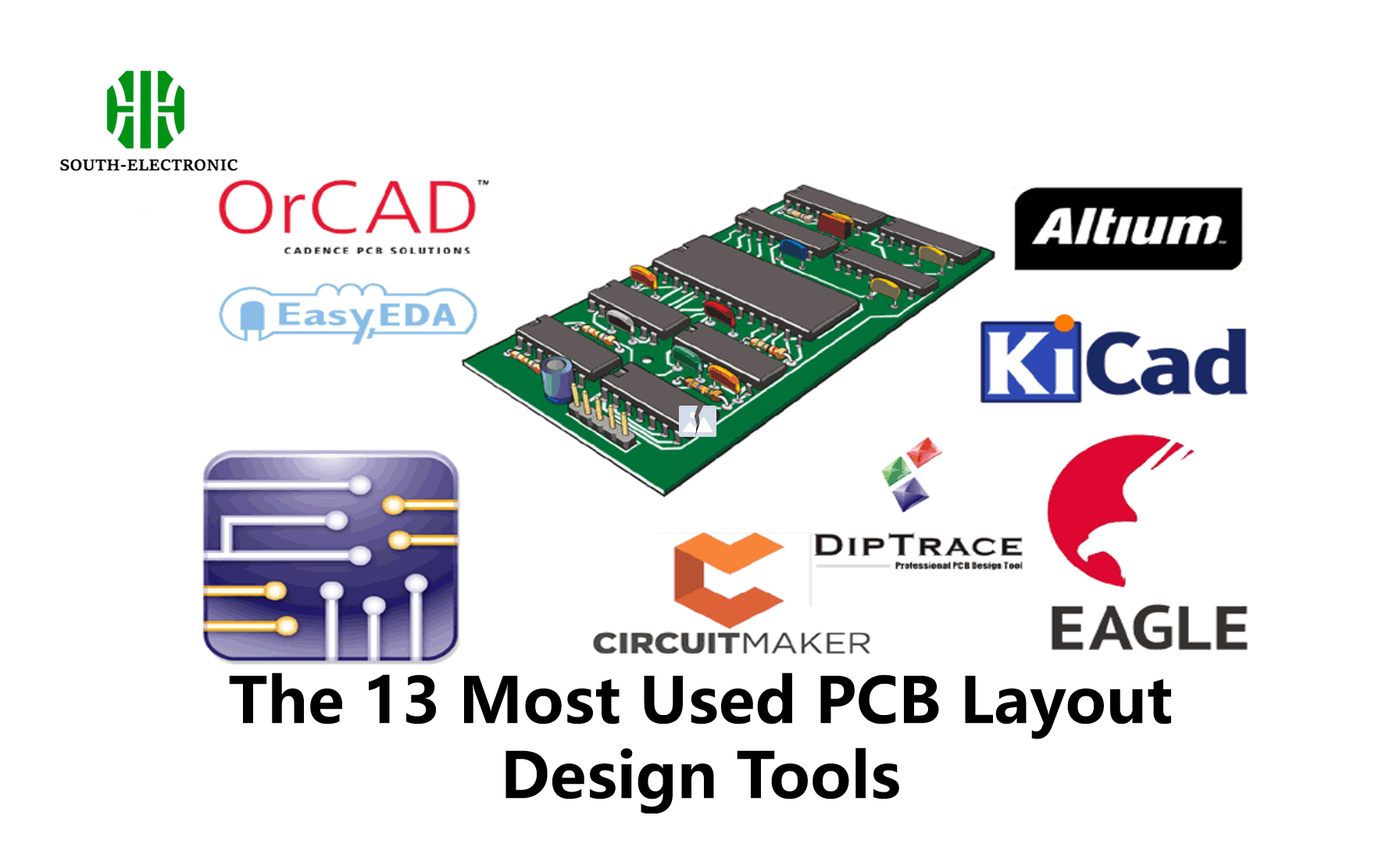
The 13 most used PCB layout design tools are Altium Designer, Eagle, KiCad, OrCAD, DipTrace, EasyEDA, ExpressPCB Plus, Siemens EDA (Mentor Graphics PADS), Siemens Xpedition, Zuken CADSTAR, Zuken CR-8000, DesignSpark, and CircuitMaker. These tools offer a range of features that cater to different user needs, from simple designs to complex, multi-layered PCB layouts.
Let’s explore each of these tools in detail to understand their unique features and how they can benefit your PCB design process.
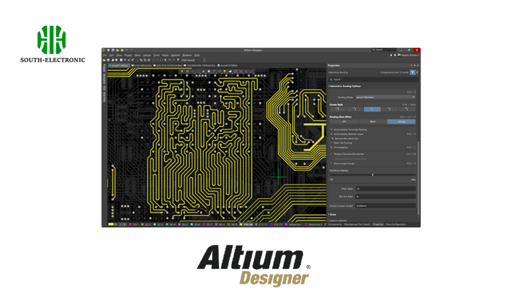
Altium Designer
Overview:Altium Designer is renowned for its unified design environment.
Features:
- Advanced routing
- 3D visualization
- Real-time BOM management
User Insights:Widely used in the industry for complex designs.
Pros and Cons:
| Pros | Cons |
|---|---|
| Extensive features | High cost |
| Excellent support | Steep learning curve |
Eagle
Overview:
Eagle is popular for its user-friendly interface and powerful features.
Features:
- Schematic capture
- PCB layout
- Auto-router
User Insights:Ideal for hobbyists and small-scale projects.
Pros and Cons:
| Pros | Cons |
|---|---|
| Affordable | Lacks advanced simulation tools |
| Easy to learn | Limited free version |
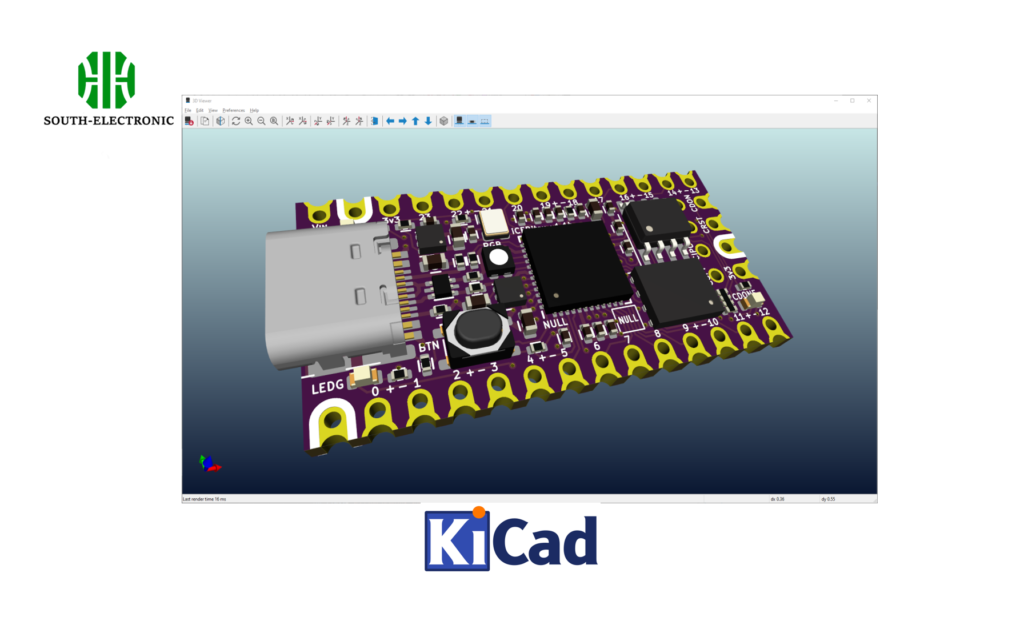
KiCad
Overview:KiCad is an open-source tool with a strong community backing.
Features:
- Multi-layer PCB support
- 3D viewer
- Schematic editor
User Insights:Great for those looking for a free yet powerful design tool.
Pros and Cons:
| Pros | Cons |
|---|---|
| Free to use | Steep learning curve |
| Robust features | Inconsistent UI |
OrCAD
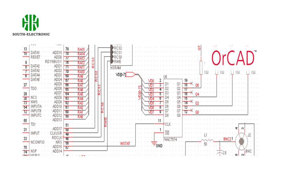
Overview:OrCAD is known for its powerful simulation capabilities.
Features:
- Advanced simulation
- PCB layout
- Design rule checks
User Insights:Preferred by professionals for high-precision designs.
Pros and Cons:
| Pros | Cons |
|---|---|
| Excellent simulation tools | Expensive |
| Precision design | Complex setup |
DipTrace
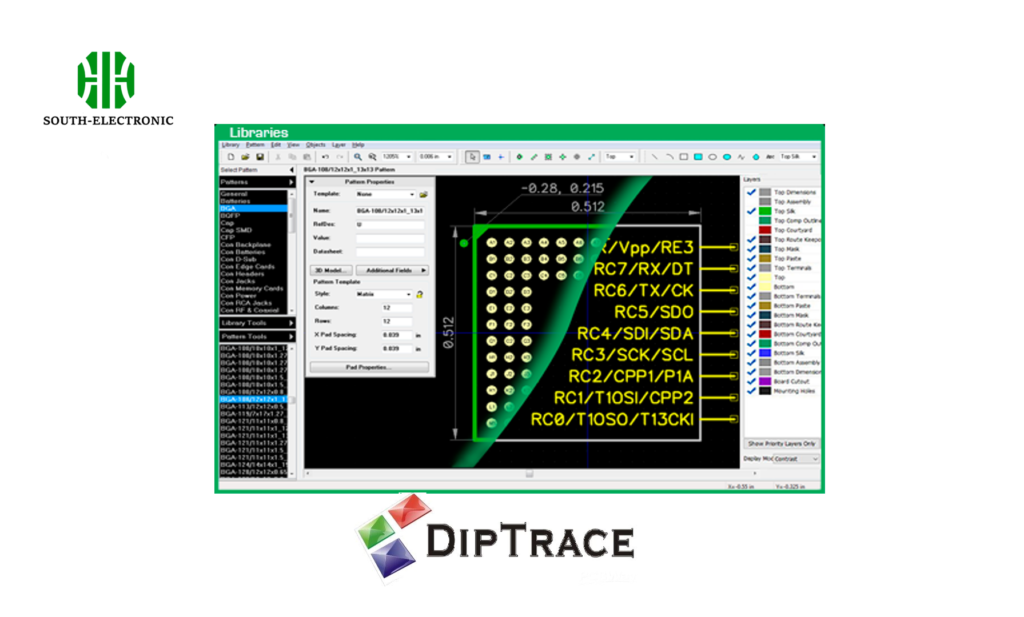
Overview:DipTrace offers an intuitive interface with strong support.
Features:
- Schematic capture
- PCB layout
- 3D preview
User Insights:Suitable for both beginners and experienced designers.
Pros and Cons:
| Pros | Cons |
|---|---|
| Easy to use | Limited advanced features |
| Strong support | Costly for high-end versions |
EasyEDA
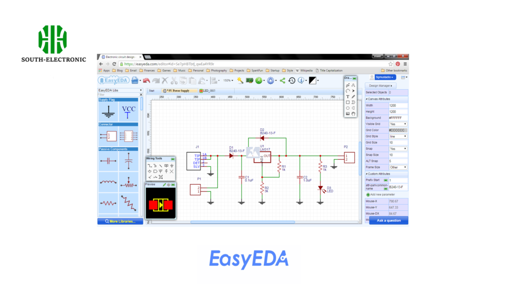
Overview:EasyEDA is a cloud-based tool that integrates with online ordering.
Features:
- Schematic capture
- PCB layout
- SPICE simulation
User Insights:Convenient for quick, collaborative projects.
Pros and Cons:
| Pros | Cons |
|---|---|
| Free version available | Cloud dependency |
| User-friendly | Limited offline capabilities |
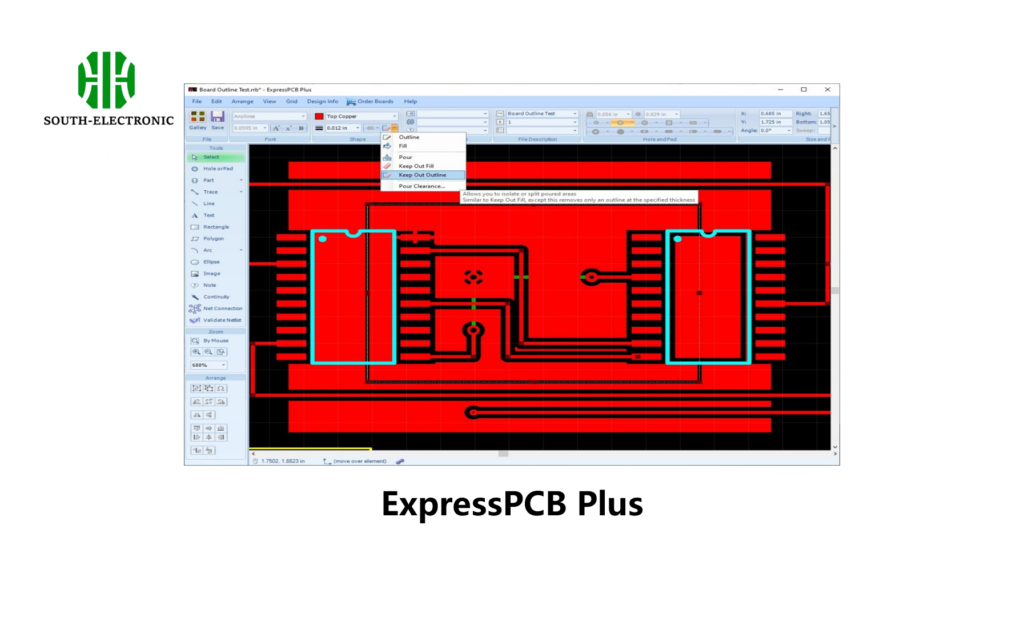
ExpressPCB Plus
Overview:ExpressPCB Plus is known for its simplicity and quick turnaround.
Features:
- Schematic capture
- PCB layout
User Insights:Ideal for rapid prototyping and simple designs.
Pros and Cons:
| Pros | Cons |
|---|---|
| Very user-friendly | Limited advanced features |
| Ideal for rapid prototyping | Basic toolset |
Siemens EDA (Mentor Graphics PADS)
Overview:Siemens EDA offers a comprehensive suite for PCB design.
Features:
- High-speed design
- Simulation
- Analysis tools
User Insights:Used by large companies for complex PCB projects.
Pros and Cons:
| Pros | Cons |
|---|---|
| Highly powerful and versatile | Expensive |
| Robust design capabilities | Steep learning curve |
Siemens Xpedition
Overview:Siemens Xpedition is designed for enterprise-level PCB design.
Features:
- Advanced routing
- Verification
- Data management
User Insights:Preferred for large-scale, multi-layer designs.
Pros and Cons:
| Pros | Cons |
|---|---|
| Unparalleled capabilities | High cost |
| Best for large-scale designs | Complex interface |
Zuken CADSTAR
Overview:CADSTAR offers a balance of power and usability.
Features:
- Schematic capture
- PCB layout
- Library management
User Insights:Suitable for medium to large projects.
Pros and Cons:
| Pros | Cons |
|---|---|
| Moderate cost | Can be complex |
| Strong features | Limited community support |
Zuken CR-8000
Overview:CR-8000 is aimed at multi-board and system-level design.
Features:
- Integrated design environment
- Simulation
- Analysis
User Insights:Best for system-level design and large teams.
Pros and Cons:
| Pros | Cons |
|---|---|
| Comprehensive features | Expensive |
| Best for system-level design | Steep learning curve |
DesignSpark
Overview:DesignSpark provides a free, yet feature-rich environment.
Features:
- Schematic capture
- PCB layout
- 3D visualization
User Insights:Great for hobbyists and small businesses.
Pros and Cons:
| Pros | Cons |
|---|---|
| Free to use | Some advanced features are limited |
| Great for hobbyists | Smaller community |
CircuitMaker
Overview:CircuitMaker is aimed at the maker community and startups.
Features:
- Schematic capture
- PCB layout
- Community collaboration
User Insights:Ideal for collaborative, open-source projects.
Pros and Cons:
| Pros | Cons |
|---|---|
| Free with community support | Lacks some advanced features |
| Ideal for collaborative projects | Dependence on community |
Summary
Choosing the right PCB layout design tool can significantly impact your project’s success. Whether you’re looking for advanced features or a user-friendly interface, these 13 tools offer a range of options to fit various needs and budgets. Try them out to find the perfect fit for your next PCB design project.
Feature Comparison
| Tool | Advanced Routing | 3D Visualization | Simulation | Real-time BOM Management | Cloud-based |
|---|---|---|---|---|---|
| Altium Designer | Yes | Yes | Yes | Yes | No |
| Eagle | Yes | Yes | No | No | No |
| KiCad | Yes | Yes | No | No | No |
| OrCAD | Yes | Yes | Yes | No | No |
| DipTrace | Yes | Yes | Yes | No | No |
| EasyEDA | Yes | Yes | Yes | No | Yes |
| ExpressPCB Plus | Yes | Yes | No | No | No |
| Siemens EDA | Yes | Yes | Yes | Yes | No |
| Siemens Xpedition | Yes | Yes | Yes | Yes | No |
| Zuken CADSTAR | Yes | Yes | Yes | No | No |
| Zuken CR-8000 | Yes | Yes | Yes | Yes | No |
| DesignSpark | Yes | Yes | Yes | No | No |
| CircuitMaker | Yes | Yes | No | No | Yes |
Pros and Cons Summary:
| Tool | Pros | Cons |
|---|---|---|
| Altium Designer | Extensive features, excellent support | High cost, steep learning curve |
| Eagle | Affordable, easy to learn | Lacks advanced simulation tools, limited free version |
| KiCad | Free to use, robust features | Steep learning curve, inconsistent UI |
| OrCAD | Excellent simulation tools | Expensive, complex setup |
| DipTrace | Easy to use, strong support | Limited advanced features, costly high-end versions |
| EasyEDA | Free version available, user-friendly | Cloud dependency, limited offline capabilities |
| ExpressPCB Plus | Very user-friendly, ideal for rapid prototyping | Limited advanced features, basic |
If you have any questions or need further information about PCB technologies, feel free to leave a comment below. Don’t forget to share this article if you found it useful, and stay connected for more insights into the fascinating world of electronics!

