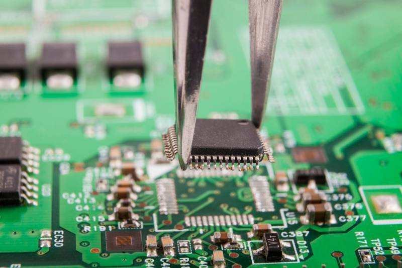
Are you struggling with overheating chips in small devices? This frustrates designers daily. The compact QFN package might solve your PCB nightmares.
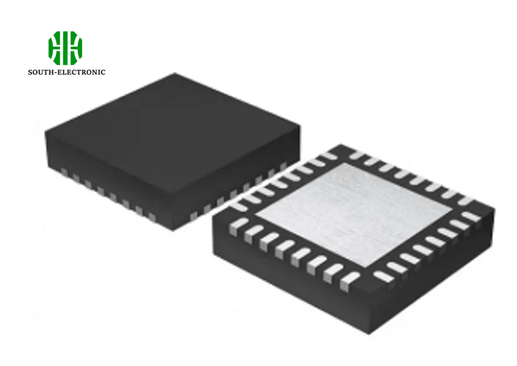
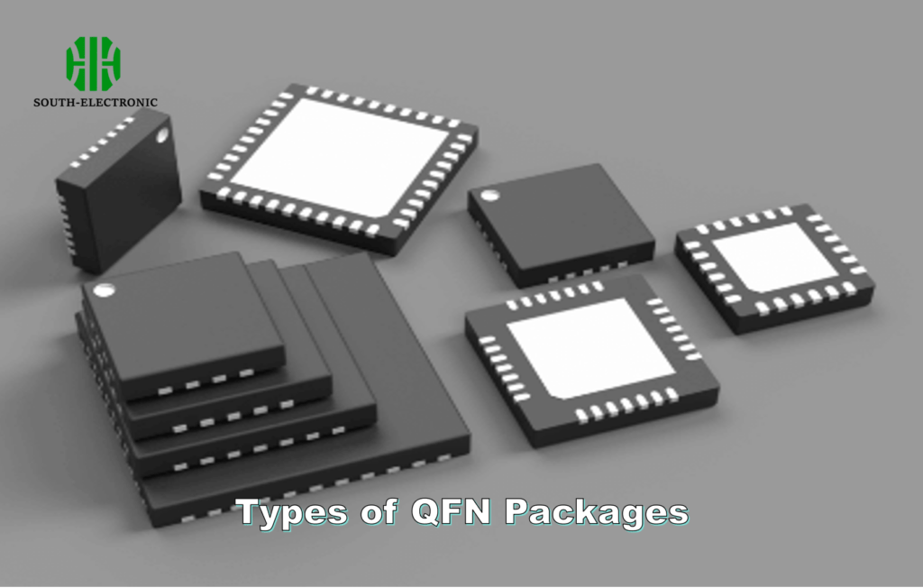
A QFN package is a leadless surface-mount IC solution offering minimal size, efficient heat dissipation via thermal pads, and superior electrical performance—ideal for lightweight electronics like smartphones and wearables.
Understanding QFN complexities is crucial. Let’s explore key comparisons and variants to upgrade your PCB design skills.
QFN vs QFP vs TQFP: How to Choose the Right Package?
Choosing wrong packages risks solder failures. Save your PCB from costly reworks by decoding differences first.
Select QFN for tiny spaces needing heat control, QFP for designs requiring manual soldering access, and TQFP for height-restricted projects with moderate pin counts.
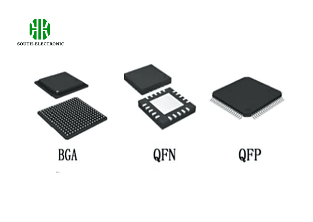
These packages differ in critical ways impacting your PCB manufacturing and performance:
Structure and Solder Attachment
| Feature | QFN | QFP | TQFP |
|---|---|---|---|
| Leads | No leads (flat pads) | Gull-wing leads | Gull-wing leads |
| Height | Thinnest (<1mm) | Moderate | Thinnest w/leads |
| Thermal Pad | Always present | Rarely included | Sometimes included |
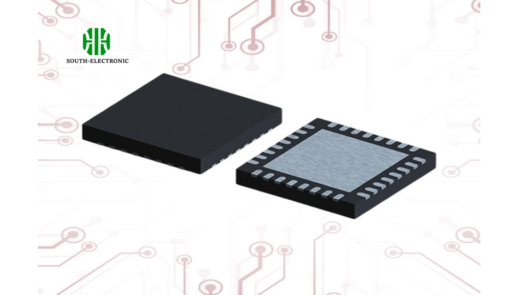
QFN packages win in space-constrained designs. The exposed copper pad underneath transfers heat directly to the PCB. This prevents overheating in compact graphics card PCBs. But there's a trade-off. Soldering QFNs requires precise reflow ovens since no leads exist.
QFPs solve hand-soldering needs. Their visible leads help manual repair work. Use them for prototypes or low-volume production. However, they consume more PCB area than QFNs.
TQFP offers middle ground. Like a flattened QFP, it suits thin devices needing moderate pin counts. But thermal performance trails behind QFN. Always check mechanical specs when using thin quad flat packages.
VQFN, LQFN, WQFN Explained: Your Guide to QFN Variants
Pick the wrong QFN variant and face hidden soldering defects. Avoid manufacturing surprises with these insights.
VQFN is ultra-thin (<0.8mm), LQFN offers standard low-profile reliability, and WQFN adds visible solder fillets for inspection—choose based on thickness needs and quality control requirements.
Deeper differences help match variants to PCB challenges:
Application-Specific Advantages
| Type | Thickness | Unique Feature | Ideal Use Case |
|---|---|---|---|
| VQFN | <0.8 mm | Extreme slimness | Smart watches, medical implants |
| LQFN | 0.8-1.4 mm | Cost-effective standard | Consumer gadget PCBs |
| WQFN | Varies | Wettable side flanks | Automotive safety systems |
VQFN fits vertically cramped spaces. Think tiny fitness trackers needing GPU-like processing power. But ultra-thin packages risk board flex damage during assembly.
LQFN provides reliable everyday usage. They work well in dashboard cameras or IoT sensors. The standard thickness makes them affordable for mass production.
WQFN solves solder verification headaches. Its metalized side surfaces create visible solder connections. This enables automated optical inspection in complex PCBs like server GPUs. The "W" means you’ll detect cold joints faster while maintaining the no-lead quad flat structure.
DFN vs QFN: Key Differences in Compact IC Packaging
Mixing DFN and QFN footprints breaks PCB layouts. Prevent assembly disasters by distinguishing their terminal patterns.
DFN packages have terminals only on two sides making them smaller, while QFN utilizes all four edges allowing more pins and better heat spreading in tight PCB areas.
Critical differentiators impact PCB real estate and functionality:
Electrical and Physical Trade-offs
| Factor | DFN Package | QFN Package |
|---|---|---|
| Pin Count | Lower density | Higher density |
| Shape | Rectangular | Square or near-square |
| Heat Flow | Moderate dissipation | Excellent via center pad |
| PCB Routing | Simpler 2-side traces | Complex 4-layer planning |
DFN packaging suits minimal I/O devices like simple sensors. Its dual-side terminals save PCB space compared to quad flat layouts. I’ve used 8-pin DFN chips in tiny RF modules successfully.
But pin constraints hit DFNs hard. Complex GPU PCBs need hundreds of connections. Here QFN wins with perimeter pin arrangements.
Thermal performance separates them too. QFN’s central thermal pad beats DFN’s smaller pads when cooling graphics card processors. Always verify thermal pad dimensions in datasheets before PCB copper pours.
Conclusion
Choose surface mount packages wisely: QFN offers ideal heat dissipation and density for modern electronics. Master its types to optimize your PCB designs.