Everyone who studies PCB design must learn design software. Whether it is Allegro or other PCB design software such as AD, mastering and using it is a basic skill that PCB engineers must have. Today, I will continue to share with you some practical tips for Allegro software.
Allegro device cannot be moved
In Allegro, Symbols have two forms of fix, they are:
-
Properties attached to symbol.
-
Inherited properties attached to symbol.
Sometimes you will find that you can’t move the device anyway. You can’t see the move option when you right-click. You can see that the fix option indicates that it is not fixed, but the prompt box will say that it is fixed. Why is this the case?
The reason is: the device inherits the fix property. This form of fix cannot be simply removed by right-clicking unfix!
Solution:
-
Without selecting any symbol, click the unfix button;
-
Then click the blank space of the symbol of the device you want to process (if you are not sure about the processing object, you can find it first through the find function);
-
Finally, done is completed.
It’s that simple!
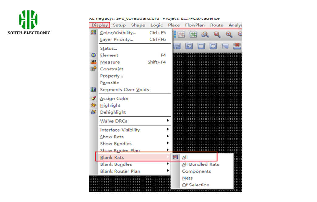
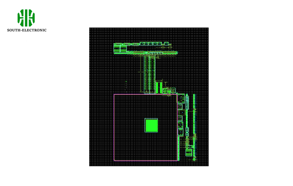
How to display and hide flying lines in Allegro?
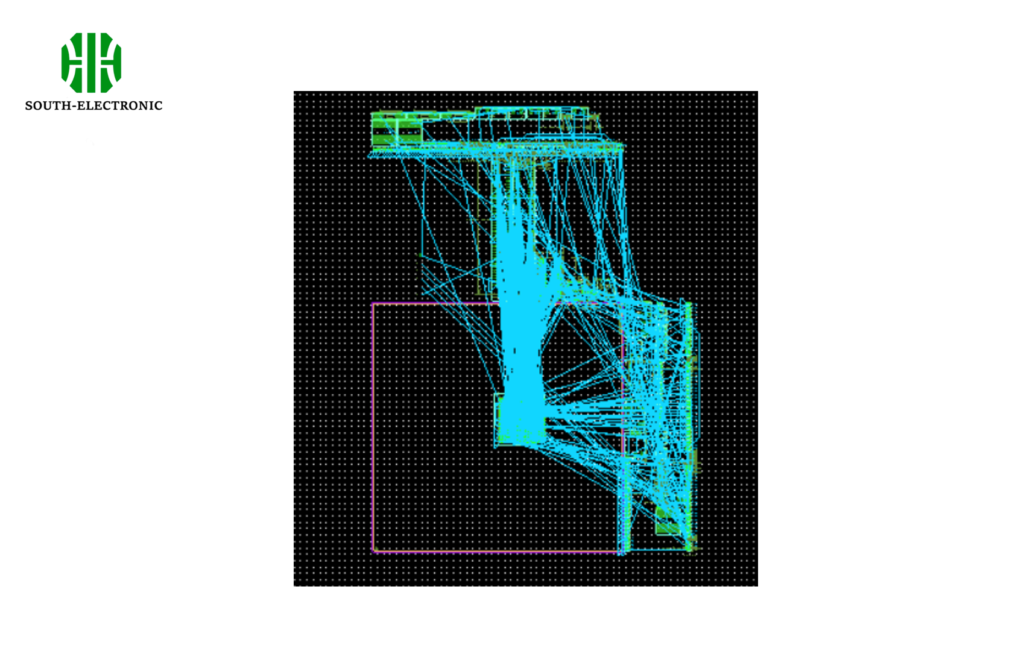
When laying out the PCB, the flying lines that are prompted are really hard to see, and you don’t know how to lay out the wiring, so you usually hide the flying lines that are prompted first, and then lay out the components.
- Hide flying lines
Settings
The effect after hiding
- Show flying lines
Settings:
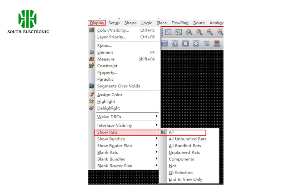
The effect of showing flying lines
Allegro deletes dangling lines
After the PCB wiring is completed, an important check is to check whether there are extra hanging lines and vias. Check through the dangling lines, vias and Antenna Report items in Tools-Quick reports. Generally speaking, we only need to pay attention to the first two items, and the third item does not need to be considered too much. It is not necessary to remove it, and the cost is very high.
Here is a simple method to remove dangling lines. You don’t need to search and delete cline segs bit by bit: route——Gloss——parameters
Click the line smoothing task in the pop-up option window, then click OK, and then click gloss to eliminate the dangling line.
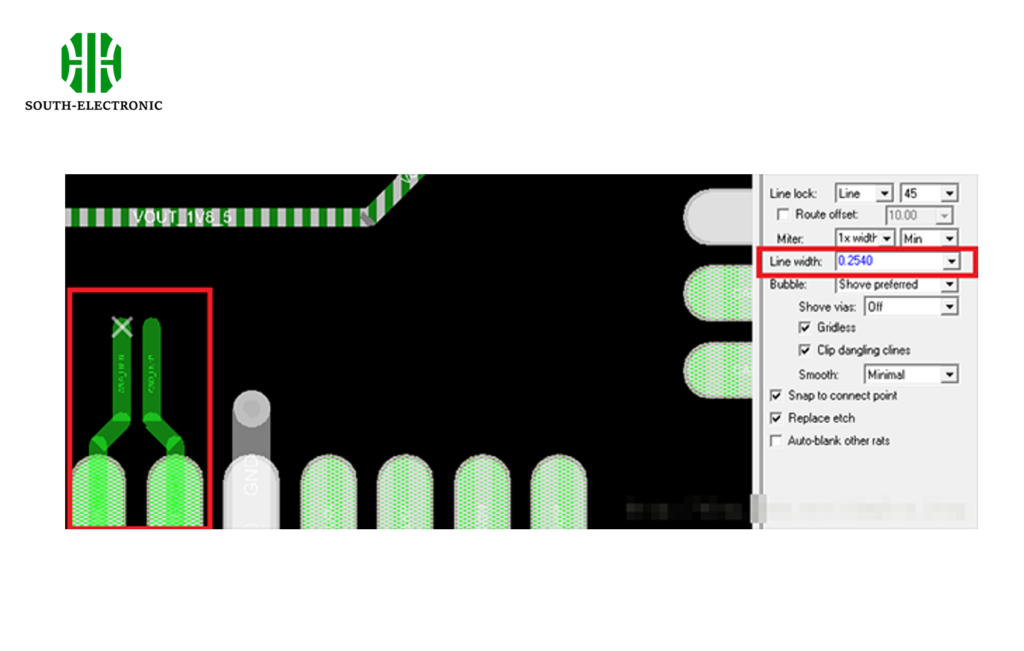
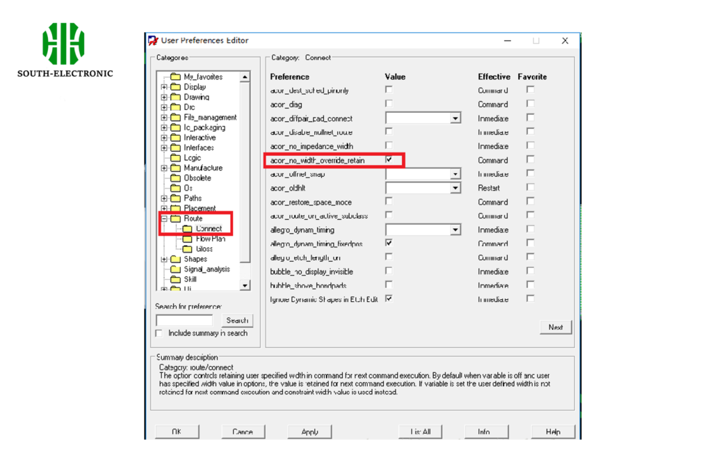
Cancel the routing memory function
In Allegro PCB, we may often switch the routing line width, but Allegro PCB remembers the routing line width by default, which means that when connecting a new network line, the software will default to the line width used to connect to the previous network. The headache I encountered was that the power line needed to be widened, but when laying the signal line, the default line width of the power supply was also used, so the line width needed to be manually modified.
Setting method: Open Allegro PCB software, select ‘Setup’–>’User Preferences’ in the menu bar, select ‘Route’–>’Connect’ on the left side of the pop-up window, and check the Value box behind ‘acon_on_width_override_retian’. As shown below:
The modified effect is as follows. The default line width of the differential pair is 0.127mm. Here I use a line width of 0.254mm to lay out this set of differential pairs. When laying out the next set of differential pairs, the software will default to the default line width of 0.127mm set in the constraint manager instead of the 0.254mm line width used last time.