In 2024, the advanced packaging market is projected to reach approximately $32.64 billion, with expectations to grow to $45 billion by 2029, reflecting a CAGR of 6.63%. This growth underscores the increasing demand for high-performance PCBs in advanced packaging applications.
South-Electronic
- Company name: South-Electronic
- Location: Suzhou, Jiangsu, China
- Company type: Electronics manufacturing and PCB assembly
- Year founded: 2001
- The number of employees: Approximately 8,000
- Main product: Printed Circuit Boards (PCBs) and advanced packaging solutions
- Other products: PCB assembly, flexible PCBs, rigid-flex PCBs, and automotive electronics components
- Company’s official website: www.south-electronic.com
Profile:
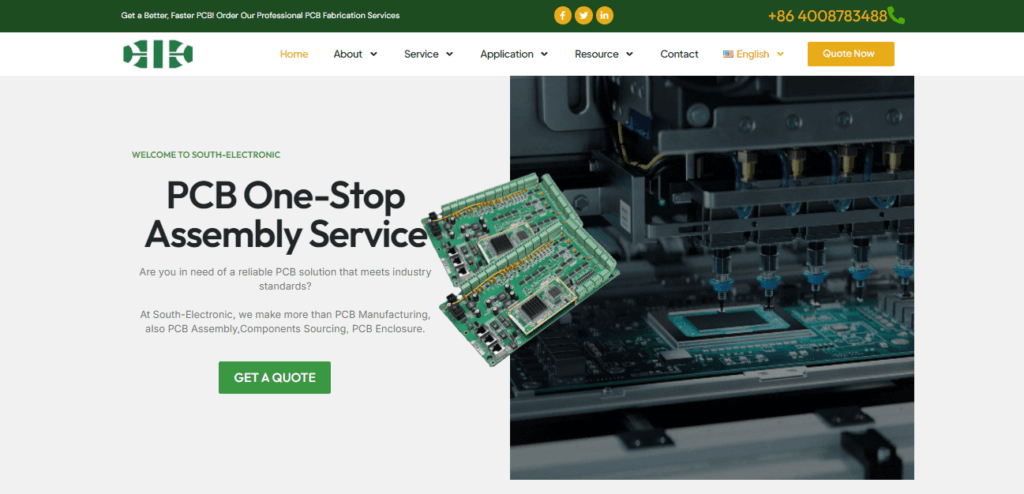
South-Electronic is a top PCB manufacturer in Suzhou, China that focuses on advanced packaging solutions for the electronics industry. They’ve been around since 2001 and have built a reputation for making high-quality PCBs and offering PCB assembly services. They work with industries like automotive, telecommunications, and consumer electronics and use the latest manufacturing technologies. They’re known for their innovations in advanced packaging technologies like wafer-level packaging (WLP), fan-out wafer-level packaging (FO-WLP), and System-in-Package (SiP).
Products and Business:
South-Electronic makes high-performance printed circuit boards (PCBs) with advanced packaging capabilities, including flexible, rigid-flex, and automotive-grade PCBs. Their products are designed for cutting-edge applications in telecommunications, automotive electronics, and consumer products. They’re also known for their precision and reliability in PCB assembly and high-tech packaging solutions.
Amkor Technology
- Company name: Amkor Technology
- Location: Tempe, Arizona, USA
- Company type: Semiconductor packaging and testing services
- Year founded: 1968
- The number of employees: Approximately 30,000
- Main product: Advanced semiconductor packaging solutions
- Other products: Wafer-level packaging, System-in-Package (SiP), flip-chip packaging, and test services
- Company’s official website: www.amkor.com

Profile:
Amkor Technology is one of the world’s largest providers of outsourced semiconductor packaging and test services. Founded in 1968, Amkor pioneered the outsourcing of IC packaging and test, and is now a strategic manufacturing partner for more than 250 of the world’s leading semiconductor companies and electronics OEMs. Amkor’s operational base includes production facilities, product development centers and sales and support offices located in key electronics manufacturing regions in Asia, Europe and the United States.
Products and Business:
Amkor provides a complete set of services to help customers manage the entire semiconductor packaging and test supply chain. These services include IC package design, package assembly, wafer probe and final test. Amkor’s strategic manufacturing capabilities enable it to offer customers a wide range of package formats and sizes, from traditional leadframe packages to advanced system-in-package (SiP) solutions. Amkor also provides semiconductor testing services for both wafer sort and final test, and offers several advanced test services such as wafer-level burn-in, wafer-level chip scale packaging and mixed-signal testing.
JCET Group
- Location: 275 Middle Binjiang Road, Jiangyin, Jiangsu Province, China
- Company type: Semiconductor packaging and testing services
- Year founded: 1972
- Number of employees: Approximately 19,812 (as of 2023)
- Main product: Advanced semiconductor packaging solutions
- Other products: Wafer-level packaging, System-in-Package (SiP), flip-chip packaging, wire bonding, and testing services
- Company’s official website: www.jcetglobal.com
Profile: JCET Group Co., Ltd., founded in 1972, is China’s largest Outsourced Semiconductor Assembly and Test (OSAT) provider and ranks third globally. The company offers comprehensive semiconductor packaging and testing services, including advanced packaging solutions such as wafer-level packaging, System-in-Package (SiP), and flip-chip technologies. With manufacturing facilities across China, Korea, and Singapore, and R&D centers in China and Korea, JCET serves a diverse clientele in industries like mobile communications, computing, consumer electronics, automotive, and industrial applications. In 2023, JCET reported revenues of approximately RMB 29.66 billion, reflecting its significant role in the semiconductor supply chain.
Products and Business: JCET specializes in advanced semiconductor packaging and testing services, including wafer-level packaging, System-in-Package (SiP), flip-chip packaging, and wire bonding. These solutions cater to sectors such as mobile communications, computing, consumer electronics, automotive, and industrial applications, emphasizing high performance and miniaturization.
Huatian Technology
- Location: No. 88, Chiyu Road, Qinzhou District, Tianshui City, Gansu Province, China
- Company type: Semiconductor packaging and testing services
- Year founded: 2003
- Number of employees: Approximately 26,427 (as of 2023)
- Main product: Advanced semiconductor packaging solutions
- Other products: System-in-Package (SiP), Through-Silicon Via (TSV), Fan-Out packaging, Wafer-Level Packaging (WLP), and testing services
- Company’s official website: www.ht-tech.com
Profile: Established in 2003, Huatian Technology is a leading semiconductor company in China, specializing in advanced packaging technologies such as System-in-Package (SiP), Through-Silicon Via (TSV), Fan-Out, and Wafer-Level Packaging (WLP). The company has expanded its global footprint by acquiring FlipChip International in the United States and Unisem in Malaysia, enhancing its capabilities in the ASEAN region. Huatian Technology has contributed to significant government projects, including the Long March 2F, Fengyun 1, Chang’e 3, Tiangong-1, and the Shenzhou series.
Products and Business: Huatian Technology offers a comprehensive range of semiconductor packaging and testing services, focusing on advanced packaging solutions like System-in-Package (SiP), Through-Silicon Via (TSV), Fan-Out, and Wafer-Level Packaging (WLP). These services cater to various industries, including consumer electronics, automotive, and telecommunications, emphasizing high performance and miniaturization.
ASE Technology
- Location: 26 Chin Third Road, Nantze Export Processing Zone, Kaohsiung 811, Taiwan, R.O.C.
- Company type: Semiconductor packaging and testing services
- Year founded: 2018 (formed through the merger of Advanced Semiconductor Engineering, Inc. and Siliconware Precision Industries Co., Ltd.)
- Number of employees: Approximately 92,000 (as of March 2024)
- Main product: Advanced semiconductor packaging solutions
- Other products: System-in-Package (SiP), Wafer-Level Packaging (WLP), front-end engineering testing, wafer probing, final testing services, and electronic manufacturing services
- Company’s official website: www.aseglobal.com
Profile: ASE Technology Holding Co., Ltd. is one of the biggest semiconductor packaging and testing services providers in the world. It was created in 2018 when Advanced Semiconductor Engineering, Inc. and Siliconware Precision Industries Co., Ltd. merged. ASE offers a range of solutions, including System-in-Package (SiP) and Wafer-Level Packaging (WLP). The company has a global presence and employs around 92,000 people. It serves clients in industries such as consumer electronics, automotive, and telecommunications. ASE is known for its commitment to quality and innovation, which has helped it become a leader in the semiconductor industry.
Products and Business:ASE specializes in advanced semiconductor packaging and testing services. It offers services such as System-in-Package (SiP), Wafer-Level Packaging (WLP), front-end engineering testing, wafer probing, final testing services, and electronic manufacturing services. These services are designed for various industries and focus on high performance and miniaturization.
TTSMC
- Location: No. 8, Li-Hsin Rd. 6, Hsinchu Science Park, Hsinchu, Taiwa
- Company type: Semiconductor manufacturing and advanced packaging services
- Year founded: 1987
- Number of employees: Approximately 65,152 (as of 2023)
- Main product: Semiconductor wafers and advanced packaging solutions
- Other products: 2.5D and 3D integrated circuit (IC) packaging, System-in-Package (SiP), and Wafer-Level Packaging (WLP)
- Company’s official website: www.tsmc.com
Profile: FTSMC is the world’s biggest semiconductor foundry, founded in 1987. They’re known for pioneering the pure-play foundry business model. TSMC has invested a lot in advanced packaging technologies, including 2.5D and 3D IC packaging. They’re a leader in the semiconductor industry because of their commitment to innovation and quality.
Products and Business: TTSMC specializes in semiconductor wafer manufacturing and advanced packaging services. They offer 2.5D and 3D IC packaging, System-in-Package (SiP), and Wafer-Level Packaging (WLP). These solutions are used in a variety of industries and focus on high performance and miniaturization.
Samsung Electronics
- Location: 129 Samsung-ro, Yeongtong-gu, Suwon-si, Gyeonggi-do, South Korea
- Company type: Electronics manufacturing, semiconductor manufacturing, and advanced packaging services
- Year founded: 1969
- Number of employees: Approximately 266,000 (as of 2023)
- Main product: Semiconductors, consumer electronics, and advanced packaging solutions
- Other products: Smartphones, televisions, home appliances, memory chips, and display panels
- Company’s official website: www.samsung.com
Profile: Founded in 1969, Samsung Electronics has evolved into a global leader in electronics manufacturing and semiconductor production. The company has made significant investments in advanced packaging technologies, offering solutions such as 2.5D and 3D packaging to meet the demands of high-performance computing. With a strong global presence and a commitment to innovation, Samsung continues to drive advancements in the semiconductor industry.
Products and Business: Samsung Electronics specializes in advanced semiconductor packaging services, including 2.5D and 3D packaging solutions. These services cater to various industries, emphasizing high performance and miniaturization.
Intel Corporation
- Location: 2200 Mission College Boulevard, Santa Clara, California, USA
- Company type: Semiconductor manufacturing and technology solutions
- Year founded: 1968
- Number of employees: Approximately 124,100 (as of 2024)
- Main product: Microprocessors and semiconductor chips
- Other products: Graphics processing units (GPUs), solid-state drives (SSDs), network interface controllers, and advanced packaging technologies
- Company’s official website: www.intel.com

Profile: Intel Corporation was founded in 1968 and is a global leader in semiconductor manufacturing. The company is known for its innovation in microprocessor technology and has made significant investments in advanced packaging technologies. One of its notable developments is the Foveros 3D packaging technique, which improves chip performance and energy efficiency. Intel’s commitment to innovation and quality has helped it become a leader in the semiconductor industry.
Products and Business:Intel specializes in microprocessors and semiconductor chips. It offers advanced packaging solutions, such as Foveros 3D packaging, to improve performance and energy efficiency. These technologies are used in various industries and focus on high performance and miniaturization.
AT&S
- Location: Fabriksgasse 13, 8700 Leoben, Austria
- Company type: Electronics manufacturing, specializing in high-end printed circuit boards (PCBs) and IC substrates
- Year founded: 1987
- Number of employees: Approximately 13,500 (as of 2023/24)
- Main product: High-density interconnect (HDI) PCBs
- Other products: IC substrates, flexible PCBs, and advanced packaging solutions
- Company’s official website: www.ats.net
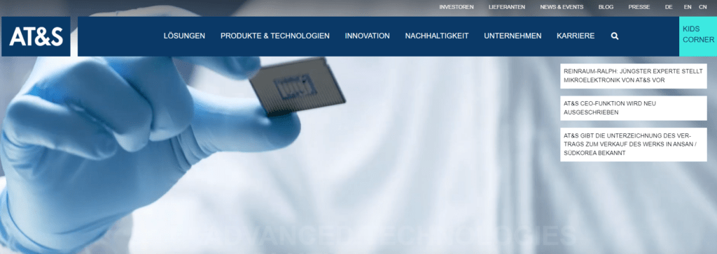
Profile: AT&S was started in 1987 and has since become a global leader in high-end PCB manufacturing, with a focus on advanced packaging solutions. The company has production sites in Europe and Asia, including Austria, China, India, Korea, and Malaysia, and employs about 13,500 people worldwide. AT&S’s technologies are used in a variety of sectors, including mobile devices, automotive, industrial, medical, aerospace, and satellites. In the 2023/24 financial year, the company had revenues of €1.55 billion, showing its importance in the electronics industry.
Products and Business: AT&S specializes in making high-density interconnect (HDI) PCBs and IC substrates, which are used in advanced packaging solutions for industries like mobile devices, automotive, industrial, medical, and aerospace. Their products are critical for high-performance and miniaturized electronic applications.
Unimicron Technology
- Location: No. 179, Shanying Road, Guishan District, Taoyuan City, 333, Taiwan
- Company type: Electronics manufacturing, specializing in printed circuit boards (PCBs) and IC substrates
- Year founded: 1990
- Number of employees: Approximately 30,320 (as of 2022)
- Main product: High-density interconnect (HDI) PCBs
- Other products: Flexible PCBs, rigid-flex PCBs, IC carriers, and testing services
- Company’s official website: www.unimicron.com

Profile: EUnimicron Technology Corporation was founded in 1990 and has since become a leading PCB manufacturer in Taiwan. The company specializes in high-precision PCBs and IC substrates for advanced packaging applications. Unimicron has manufacturing sites and service centers in Taiwan, China, Germany, and Japan, and serves customers worldwide. Unimicron’s products are used in a variety of applications, including LCD monitors, PCs, mobile phones, and other consumer electronics. The company’s commitment to innovation and quality has made it a leader in the PCB industry.
Products and Business: Unimicron manufactures HDI PCBs, flexible PCBs, rigid-flex PCBs, and IC carriers. These products are used in industries such as consumer electronics, automotive, and telecommunications, and are designed for high performance and miniaturization.
If you’re still searching for the right manufacturer for advanced packaging PCBs, consider South-Electronic. With our expertise in high-quality production, tailored solutions, and reliable global support, we’re here to meet your advanced packaging needs efficiently and cost-effectively.

