
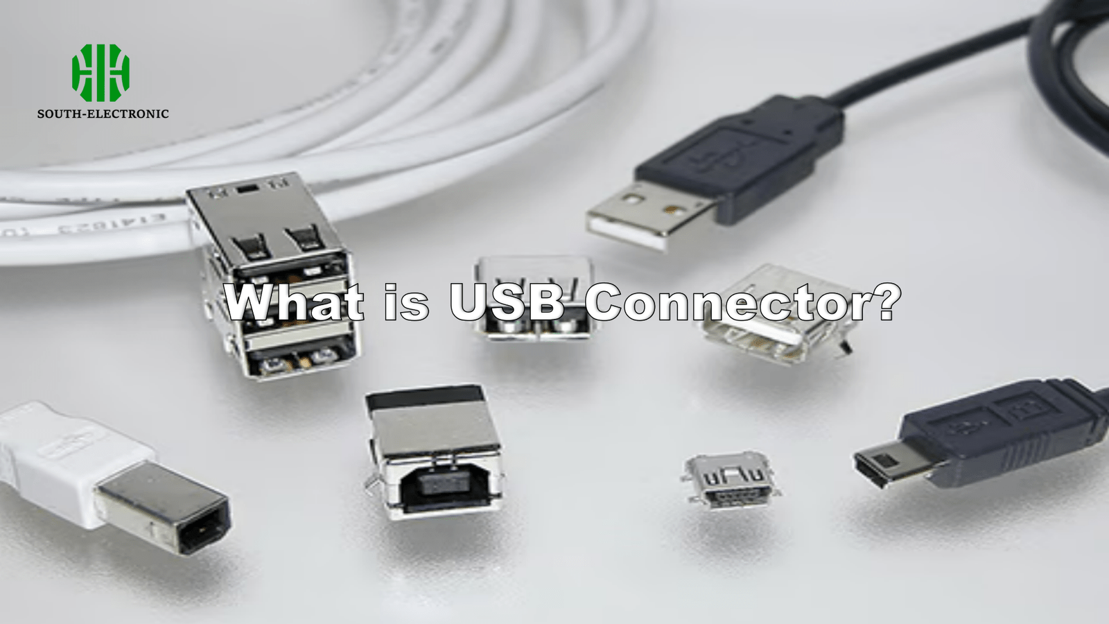
Have you ever struggled with plugging in USB cables upside-down? This 4×10mm wonder solves that while powering our digital world. Let’s dissect this engineering miracle.
A USB connector[^1] is a standardized interface for transferring data and power between devices through metallic contacts and insulated housing. Modern versions like USB-C[^2] feature reversible designs supporting up to 40Gbps data transfer and 240W power delivery[^3].
)
From ancient USB-A ports to modern multi-functional connectors, this technology’s evolution reveals surprising engineering choices. We’ll examine four critical aspects shaping today’s USB designs.
Core Structure: Pins, Housing & Shielding Explained?
That satisfying click when inserting USB cables comes from precise mechanical engineering. Let’s decode the hidden layers of this ubiquitous connector.
Key structural components include gold-plated contact pins for signal transmission, molded polymer housing for insulation, and stainless steel shielding against electromagnetic interference. The number of pins varies from 4 (USB 2.0) to 24 (USB4).
)
Understanding Contact Matrix
| Component | USB-A (2.0) | USB-C (3.2) | Function |
|---|---|---|---|
| VBus Pin | 1 | 4 | Power delivery (5-48V) |
| Ground Pin | 1 | 4 | Electrical return path |
| D+/D- Pairs | 2 | 2 | USB 1.1/2.0 data transfer |
| TX/RX Pairs | 0 | 8 | High-speed differential |
| CC Pin | 0 | 2 | Connection configuration |
The contact arrangement directly determines capabilities. USB-C’s 24-pin layout enables bidirectional power delivery and dual-lane data transmission. Newer USB4 versions use the same pins but with advanced protocol tunneling. Shielding effectiveness drops from 85dB at 1GHz to 60dB at 5GHz, showing increasing interference challenges.
PCB Integration: Soldering Techniques & Signal Integrity
Why do some USB ports wobble while others last years? The answer lies beneath the solder joints.
Surface-mount technology (SMT)[^4] allows 0.4mm pitch soldering for compact designs, while through-hole variants offer mechanical strength. Proper impedance control (90Ω ±15%) prevents signal reflection in high-speed USB3.2/4.0 implementations.
)
Termination Methods Comparison
| Parameter | Wave Soldering | Reflow Soldering | Selective Soldering |
|---|---|---|---|
| Process Temp | 260°C | 230-250°C | 300°C |
| Cycle Time | 45s | 5-7min | 15s/joint |
| Solder Thickness | 2-4μm | 3-5μm | 1-3μm |
| Cost/Unit | $0.02 | $0.05 | $0.08 |
| Best For | Through-hole | SMT | Mixed assemblies |
Lead-free SAC305 solder (96.5% Sn, 3% Ag, 0.5% Cu) dominates modern production. Solder joint cracks account for 72% of USB port failures. Reflow profiling critical – peak temperatures must stay within 235-245°C range to prevent pad lifting.
Three Major Technological Changes in USB PCB
From copper thickness to dielectric materials, USB evolution demands PCB innovations.
Key advancements include: 1) 6-layer stackups with 0.1mm microvias for USB4 routing, 2) Low-loss substrates like Megtron6[^5] (Dk=3.7 @10GHz), 3) Embedded USB power controllers reducing component count by 40%.
)
Material Property Evolution
| Generation | FR4 Standard | High-Speed FR4 | Rogers 4350B |
|---|---|---|---|
| Df @1GHz | 0.020 | 0.005 | 0.0037 |
| Dk | 4.5 | 3.8 | 3.66 |
| Cost | $1.2/sqft | $3.8/sqft | $12/sqft |
| CTE (ppm) | 14 | 12 | 11 |
Contentious transition underway – standard FR4 can’t handle USB4’s 20GHz signals. Cutoff frequency (fc) calculation: fc = c/(2π√εr)·(1/tr). For USB4’s 0.5ns rise time, fc ≈7GHz. Material selection now impacts EMI certification success rates.
Conclusion
USB connectors exemplify miniaturized engineering – from atomic-level gold plating to macroscopic mechanical reliability. Next plug-in, appreciate the hidden complexity!
[^1]: Explore this link to understand the various USB connector types and their specific applications, enhancing your tech knowledge.
[^2]: Discover the benefits of USB-C, including its speed and versatility, which are crucial for modern devices.
[^3]: Learn about USB power delivery technology and its advantages for charging devices efficiently and quickly.
[^4]: Explore the benefits of SMT in PCB design, including compactness and efficiency, to enhance your understanding of modern electronics.
[^5]: Discover how low-loss substrates like Megtron6 improve signal integrity in high-speed applications, crucial for advanced PCB designs.


