
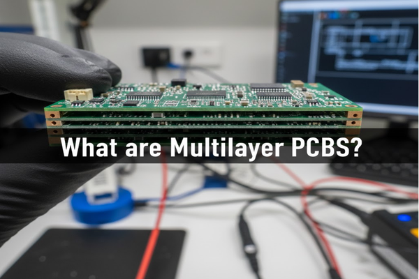
Do complex electronics give you a headache? Need more power and smaller size for your circuits? Multilayer PCBs are the answer you've been looking for.
Multilayer PCBs[^1] are circuit boards with three or more conductive copper layers[^2] stacked together[^3], separated by insulating materials[^4]. They are pressed under heat and pressure into a single, compact unit, allowing for much more complex and dense electronic designs.
I remember when I first started in electronics; single-layer boards felt like magic. But as projects grew more intricate, I quickly hit a wall. That's when I discovered the incredible world of multilayer PCBs, and trust me, they changed everything.
How many layers can a PCB have?
Struggling with crowded circuit boards and limited space? Ever wonder just how many layers you can cram into a PCB to solve those issues?
A PCB can have many layers, typically ranging from 4 to over 60, though most commonly, they feature an even number like 4, 6, or 8 layers for better manufacturing stability.
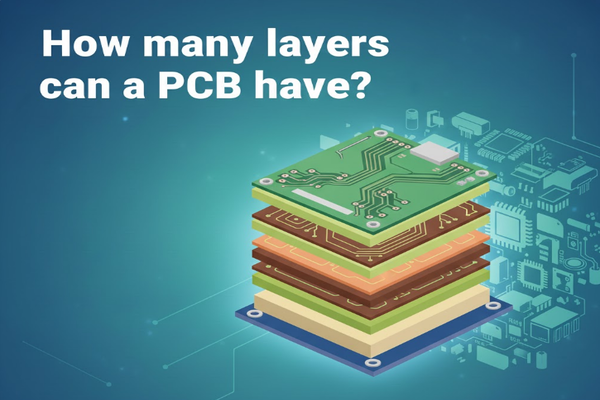
When I think about the sheer number of layers possible, it really highlights the flexibility of these boards. While the theoretical limit is high, practical applications usually stick to a more manageable range.
Understanding Layer Counts
The number of layers isn't just about fitting more traces; it's about optimizing performance.
- Standard Multilayer PCBs: Most common designs use 4, 6, or 8 layers. These offer a good balance of complexity, performance, and cost.
- High-Layer Count PCBs[^5]: Some advanced applications, like supercomputers or aerospace systems, can feature 30, 40, or even 60 layers. This allows for incredibly dense routing and specialized impedance control.
- Why Even Numbers? While technically possible to have odd-numbered layers (e.g., 3, 5), manufacturers often avoid them. An odd number of layers can lead to an unbalanced stack-up. This imbalance can cause warping during the lamination process due to uneven thermal expansion and contraction, which increases manufacturing difficulty and cost.
Common Layer Stack-ups
Different layer counts serve different purposes.
| Layers | Typical Applications | Benefits |
|---|---|---|
| 4 | Simple embedded systems, basic networking, consumer electronics | Cost-effective, good for moderate density, offers improved EMI shielding |
| 6 | Advanced consumer electronics, industrial control, medical devices | Better signal integrity[^6], more routing space, enhanced power distribution |
| 8+ | High-speed computing, telecommunications, aerospace | Excellent signal integrity, high component density, complex impedance control |
I've seen firsthand how choosing the right number of layers can make or break a project, especially when dealing with high-frequency signals. It's not just about fitting wires; it's about electrical performance.
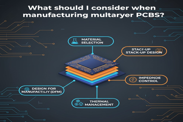
What should I consider when manufacturing multilayer PCBs?
Worried about costly mistakes in your next PCB project? Not sure how to get the best performance from a multilayer design?
When manufacturing multilayer PCBs, key considerations include material selection, stack-up design, impedance control, thermal management, and careful design for manufacturability (DFM) to ensure reliability and performance.
Designing a multilayer PCB is like building a miniature skyscraper for electronics. Every decision, from the ground floor to the penthouse, affects its stability and function. I learned this the hard way on a project where I overlooked thermal management, leading to unexpected failures.
Material Selection
The choice of materials is fundamental to the PCB's performance and reliability.
- Substrate Material (Dielectric): This insulating layer separates the conductive copper layers. Common materials include FR-4 (flame retardant type 4), which is widely used due to its good electrical properties and cost-effectiveness. For higher frequency applications, materials like high-Tg FR-4, polyimide, or specialized ceramic-filled laminates are necessary. I always consider the operating temperature and signal speed when picking these.
- Copper Weight: This refers to the thickness of the copper foil. Standard weights are 1 oz/sq ft or 2 oz/sq ft. Higher copper weights are used for power planes and high-current applications, which helps with heat dissipation.
Stack-up Design
The arrangement of layers, or "stack-up," critically influences signal integrity and EMI performance.
- Signal Layers: These layers carry the data and clock signals. They should be placed between ground planes to provide shielding and a controlled impedance environment.
- Power and Ground Planes: Dedicated planes for power and ground are essential for stable power delivery and reducing noise. These planes act as a return path for signals and help dissipate heat. I make sure to distribute them evenly for thermal balance.
- Symmetry: As I mentioned earlier, maintaining a symmetrical stack-up (e.g., core-prepreg-core) is crucial for preventing warping during manufacturing and ensuring mechanical stability.
Impedance Control
For high-speed designs, controlling impedance is non-negotiable.
- Trace Width and Spacing: These dimensions, along with dielectric thickness and material properties, determine the characteristic impedance of a trace. I use impedance calculators to ensure traces match the required impedance, often 50 ohms for single-ended signals and 100 ohms for differential pairs.
- Dielectric Constant: The dielectric constant (Er) of the chosen material directly affects impedance. Knowing and specifying this accurately to the manufacturer is vital.
Thermal Management
Heat is the enemy of electronics, and multilayer PCBs can generate a lot of it.
- Thermal Vias: These are non-electrical vias specifically designed to conduct heat away from hot components to cooler areas or heatsinks. I always add these under power-hungry ICs.
- Copper Pours and Planes: Large copper areas act as heat sinks, spreading heat across the board.
- Component Placement: Strategic placement of heat-generating components to allow for efficient heat dissipation is critical.
Design for Manufacturability (DFM)[^7]
Considering the manufacturing process early saves time and money.
- Minimum Trace Width/Spacing: Adhere to the manufacturer's capabilities to avoid increased costs or design violations.
- Via Types: Understand the different via types (through-hole, blind, buried) and their impact on cost and density. Blind and buried vias allow for higher density but are more expensive.
- Panelization: Discuss panelization options with the manufacturer to optimize board utilization and reduce per-board cost.
By carefully considering these factors, I ensure my multilayer PCB designs are not only functional but also reliable and cost-effective to produce.
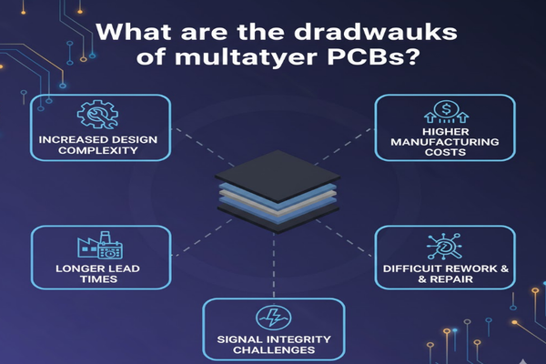
What are the drawbacks of multilayer PCBs?
Thinking multilayer PCBs are a silver bullet for all your design problems? Overlooking their downsides could lead to unexpected issues and budget overruns.
While powerful, multilayer PCBs have drawbacks including higher manufacturing costs[^8], increased design complexity, more difficult rework and repair, longer lead times[^9], and potentially greater signal integrity challenges if not designed carefully.
I've learned that every technology comes with its trade-offs. Multilayer PCBs, for all their advantages, are no exception. There was a time I jumped into a 10-layer design for a relatively simple project, only to regret the ballooning costs and development time.
Increased Cost
This is often the first and most obvious drawback.
- Material Costs: More layers mean more raw materials (copper, prepreg, core), which directly increases the bill of materials.
- Manufacturing Complexity: The lamination process, precise alignment of multiple layers, and drilling of complex vias (blind/buried) require more sophisticated equipment and more processing steps. Each additional step adds to the manufacturing cost.
- Tooling Costs: Initial tooling and setup costs can be higher due to the precision required for multilayer fabrication.
Design Complexity
As layers increase, so does the intricacy of the design process.
- Routing Challenges: While more layers offer more routing space, managing inter-layer connections and ensuring proper signal return paths becomes more complex.
- Stack-up Optimization: Designing an optimal stack-up for signal integrity, impedance control, and thermal performance requires specialized knowledge and simulation tools.
- Software Demands: Advanced CAD software and simulation tools are often necessary, which can add to design costs and learning curves.
Rework and Repair Difficulty
Once laminated, a multilayer PCB is a monolithic block.
- Accessibility: Internal layers are inaccessible. If a trace on an inner layer has an issue, repairing it is nearly impossible without damaging the entire board.
- Component Desoldering: Desoldering multi-pin components on multilayer boards can be challenging due to the increased thermal mass and heat sinking capabilities of the multiple layers, potentially damaging pads or traces. I've ruined a few boards trying to fix a single misplaced component.
Longer Lead Times
The manufacturing process for multilayer PCBs is more involved.
- Fabrication Time: The additional steps (layer preparation, lamination cycles, more drilling, plating) naturally extend the time it takes to produce the bare boards compared to single or double-sided PCBs.
- Prototyping Delays: This means that prototyping cycles can be longer, which can slow down product development.
Signal Integrity Challenges
While designed to improve signal integrity, poor design can exacerbate issues.
- Crosstalk: Without careful planning of trace spacing and shielding, signals on adjacent layers or traces can interfere with each other.
- EMI/EMC[^10]: Poor stack-up design can lead to increased electromagnetic interference (EMI) and reduced electromagnetic compatibility (EMC), requiring more shielding or filtering.
- Power Delivery Network (PDN): Ensuring a stable power supply across multiple layers and components requires careful design of power and ground planes to minimize voltage drops and noise.
Understanding these drawbacks helps in making informed decisions, ensuring that the benefits of multilayer PCBs truly outweigh their complexities for any given project.
Is South-Electronic[^11] the best PCB manufacturer in China?
Searching for the absolute best PCB manufacturer can feel overwhelming, especially with so many options in China, but are they truly the top choice?
Determining the "best" PCB manufacturer like South-Electronic depends on specific project needs, as factors such as cost, quality, lead time, communication, and specialization vary among suppliers.

I've learned that every technology comes with its trade-offs. Multilayer PCBs, for all their advantages, are no exception. There was a time I jumped into a 10-layer design for a relatively simple project, only to regret the ballooning costs and development time.
Defining "Best"
The "best" manufacturer isn't a universal title; it's a match between your needs and their strengths.
- Quality Standards: Does the manufacturer adhere to international standards like ISO 9001, UL, and RoHS? Are their quality control processes robust? Look for evidence of strict incoming material inspection and final product testing.
- Capabilities: Can they produce the specific type of PCB you need (e.g., high-layer count, HDI, flexible, rigid-flex, specialized materials)? Do they have experience with your industry's requirements (e.g., medical, automotive)?
- Cost-Effectiveness: This isn't just about the lowest price per board. It includes tooling costs, shipping, and the overall value for money, considering quality and lead time. A slightly higher price for better quality can save significant costs down the line.
- Lead Times: How quickly can they turn around prototypes and production orders? Do they offer expedited services if needed? This is critical for meeting tight development schedules.
- Communication and Support: How responsive are they to inquiries? Do they have English-speaking technical support? Clear communication is vital, especially when dealing with complex designs or potential issues.
Evaluating South-Electronic (and others)
Without specific performance metrics for South-Electronic, here's how I'd generally evaluate any Chinese manufacturer.
- Website and Certifications: A professional website detailing their capabilities and openly displaying certifications is a good start.
- Customer Reviews and References: Look for independent reviews, testimonials, or ask for references from clients in a similar industry.
- Request for Quote (RFQ) Process: How thorough and clear is their RFQ response? Do they ask intelligent questions about your design, indicating a good understanding?
- Prototyping: Start with a small prototype order[^12]. This is the best way to assess their quality, lead time, and communication before committing to large production runs. I always recommend this step.
- Factory Audit (if applicable): For larger orders, a factory audit or third-party inspection can provide deeper insights into their operations and quality control.
Conclusion
Multilayer PCBs offer advanced solutions for complex electronics, but require careful design and manufacturing consideration to balance performance with cost and complexity.
[^1]: Explore the advantages of multilayer PCBs for complex electronic designs and their impact on performance. [^2]: Learn about the role of conductive copper layers in enhancing PCB functionality and design. [^3]: Understand the process of stacking layers in PCBs and its significance in design. [^4]: Discover the various insulating materials that improve PCB performance and reliability. [^5]: Learn about the applications and benefits of High-Layer Count PCBs in technology. [^6]: Explore the concept of signal integrity and its importance in multilayer PCB design. [^7]: Learn how DFM principles can enhance PCB production efficiency and reduce costs. [^8]: Understand the various factors that contribute to the manufacturing costs of multilayer PCBs. [^9]: Explore the lead times involved in multilayer PCB manufacturing and their impact on projects. [^10]: Learn about electromagnetic interference and compatibility in PCB designs. [^11]: Evaluate the reliability and quality of South-Electronic as a PCB manufacturer. [^12]: Understand the significance of starting with a prototype order for PCB quality assessment.

