
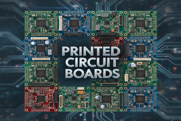
Ever wondered about the hidden brains inside your electronics? The stuff that makes them tick? PCBs are crucial, yet often overlooked, components.
Printed Circuit Boards (PCBs) are foundational platforms for electronic components[^1]. They mechanically support and electrically connect electronic components using conductive tracks[^2], pads, and other features etched from copper sheets[^3].
When I first started tinkering with electronics, I quickly realized that understanding PCBs was like unlocking a secret language. It moved me past just seeing blinking lights to truly grasping how devices function. Join me as we peel back the layers of these essential components.
How are PCBs Made?
Curious how those intricate green boards come to life? From raw materials to finished product, the PCB manufacturing process is a marvel of engineering.
PCBs are made through a complex process involving etching copper, drilling holes, plating, and laminating layers. This multi-step manufacturing creates the precise pathways needed for electronic signals.
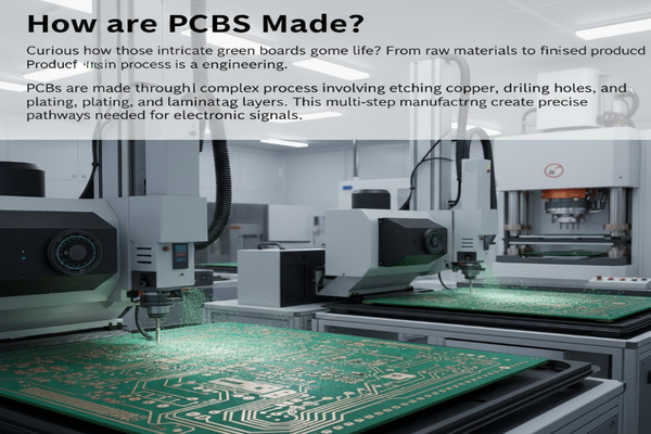
The creation of a PCB is a highly precise and multi-layered process. It starts with a substrate material[^4], often fiberglass, coated with copper. Here’s a breakdown:
Core Steps in PCB Fabrication
- Design & Layout:
- CAD Software[^5]: Engineers use Computer-Aided Design (CAD) software to create the circuit layout.
- Gerber Files[^6]: This design translates into Gerber files, which are blueprints for manufacturing.
- Material Preparation:
- Substrate Selection: Choosing the right base material (e.g., FR-4 for rigidity, flexible polyimide for flexibility).
- Copper Cladding: Applying copper layers to the substrate.
- Imaging & Etching:
- Photoresist Application: A photosensitive film is applied to the copper.
- UV Exposure: The design is transferred onto the photoresist using UV light.
- Etching: Unwanted copper is removed chemically, leaving the circuit traces.
- Drilling & Plating:
- Hole Drilling: Precisely drilling holes for component leads and vias (interlayer connections).
- Electroless Plating: Depositing a thin layer of copper into the holes.
- Electroplating: Building up copper thickness in the holes and on traces.
- Solder Mask & Silkscreen:
- Solder Mask: Applying a protective layer (usually green) to prevent solder bridges.
- Silkscreen: Printing component identifiers, logos, and reference designators.
- Finishing & Testing:
- Surface Finish: Applying a surface finish (e.g., HASL, ENIG) to protect exposed copper.
- Electrical Test: Verifying continuity and isolation of all circuits.
| Step | Description | Key Material / Tool |
|---|---|---|
| Design | Circuit layout creation | CAD Software |
| Etching | Removing unwanted copper | Photoresist, Etchant |
| Drilling | Creating holes for components and vias | CNC Drills |
| Plating | Electrically connecting layers | Copper, Electrolytes |
| Solder Mask | Protecting traces, preventing shorts | Epoxy-based polymer |
| Silkscreen | Component labeling | Ink, Screen printing |
| Final Test | Verifying electrical functionality | Flying Probe Tester |
Who is Involved in Printed Circuit Board Design?
Designing a PCB isn't a solo act. It's a collaborative effort requiring diverse skills. Who are these unsung heroes behind the scenes?
PCB design involves a team of specialists: electrical engineers for schematics, layout engineers for physical placement, and mechanical engineers for enclosure fit. Their collaboration ensures a functional and manufacturable board.
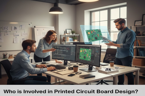
When I first started out, I thought design was just one person drawing lines. I quickly learned that it's far more complex. A successful PCB project brings together a range of expertise to ensure everything from the smallest resistor to the overall power distribution works perfectly.
Key Roles in PCB Design and Development
- Electrical Engineer:
- Responsibility: Focuses on the circuit's functionality and performance.
- Tasks: Creates the schematic diagram, selects components, performs simulations, and defines electrical specifications. They determine what the circuit needs to do.
- PCB Layout Engineer (or Designer):
- Responsibility: Translates the electrical schematic into a physical layout.
- Tasks: Places components, routes traces, manages signal integrity, ensures manufacturability, and considers thermal management. They determine how the circuit fits on the board.
- Mechanical Engineer:
- Responsibility: Ensures the PCB fits within its physical enclosure and interacts correctly with other mechanical parts.
- Tasks: Designs the enclosure, verifies mounting points, considers vibration and environmental protection, and checks connector alignment.
- Firmware/Software Engineer:
- Responsibility: Develops the code that runs on the microcontrollers or processors on the PCB.
- Tasks: Programs embedded systems, writes drivers for peripherals, and ensures the software interacts correctly with the hardware.
- Test Engineer:
- Responsibility: Designs and implements testing procedures to verify the PCB's functionality and reliability.
- Tasks: Develops test jigs, writes test scripts, and performs functional and in-circuit tests.
- Manufacturing Engineer:
- Responsibility: Bridges the gap between design and production, ensuring the PCB can be efficiently mass-produced.
- Tasks: Advises on design for manufacturability (DFM) and design for assembly (DFA), optimizes production processes, and troubleshoots manufacturing issues.
| Role | Primary Focus | Key Output |
|---|---|---|
| Electrical Engineer | Circuit functionality | Schematic Diagram |
| PCB Layout Engineer | Physical board arrangement | Gerber Files, Board Layout |
| Mechanical Engineer | Enclosure & fit | Mechanical CAD drawings |
| Firmware Engineer | Embedded software | Code, Firmware |
| Test Engineer | Quality & reliability | Test Plans, Test Reports |
| Manufacturing Engineer | Production efficiency | DFM/DFA Feedback |
Where are Printed Circuit Boards Used?
Look around you. Chances are, a PCB is making that device work. From tiny wearables to massive industrial machines, their reach is vast.
PCBs are ubiquitous in modern electronics, forming the core of almost every electronic device. They enable functionality in consumer gadgets, industrial machinery, medical equipment, and communication systems worldwide.
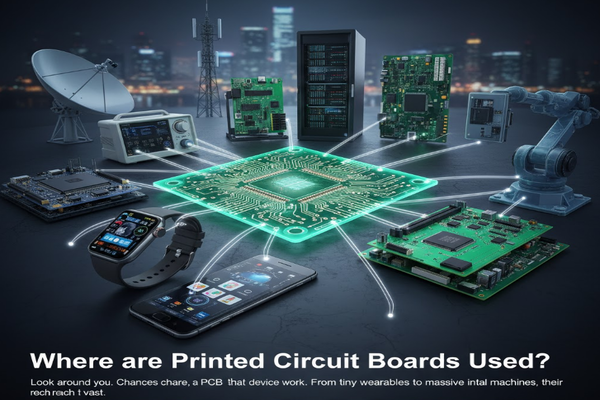
My fascination with PCBs grew when I realized they weren't just in my computer, but everywhere! They are truly the unsung heroes of our interconnected world, silently enabling everything from our morning coffee maker to complex space missions.
Common Industries and Applications for PCBs
- Consumer Electronics:
- Description: This is probably the most obvious category. Every smartphone, laptop, smart TV, gaming console, and even your smart home devices rely heavily on PCBs. They handle everything from basic power distribution to complex processing tasks.
- Examples: Motherboards in computers, display drivers in TVs, control boards in washing machines.
- Automotive Electronics[^7]:
- Description: Modern cars are essentially computers on wheels. PCBs are vital for engine control, safety systems (ABS, airbags), infotainment, LED lighting, advanced driver-assistance systems (ADAS), and even electric vehicle battery management.
- Examples: Engine Control Units (ECUs), dashboard displays, GPS systems, sensor arrays.
- Aerospace and Defense:
- Description: In environments where reliability is paramount, high-performance PCBs are used in avionics, radar systems, satellite communication, and missile guidance. These often require specialized materials and robust designs.
- Examples: Flight control systems, satellite transponders, military communication devices.
- Medical Devices[^8]:
- Description: The precision and reliability required for medical equipment make PCBs indispensable. They are found in diagnostic imaging, patient monitoring, surgical tools, and implantable devices.
- Examples: MRI and CT scanners, pacemakers, glucose meters, ultrasound equipment.
- Industrial and Power Electronics:
- Description: From factory automation to energy management, PCBs control industrial machinery, robotics, power supplies, and renewable energy systems. They need to withstand harsh conditions and handle high power.
- Examples: PLC controllers, motor drives, solar inverters, industrial robotics.
- Telecommunications:
- Description: The infrastructure of our global communication network relies on PCBs. They are in routers, switches, cellular base stations, and fiber optic systems, facilitating data transfer.
- Examples: Server boards, network interface cards, base station transceivers.
| Industry | Key Applications | PCB Characteristics (General) |
|---|---|---|
| Consumer Electronics | Smartphones, Laptops, TVs, Wearables | High density, low cost, small form factor |
| Automotive Electronics | ECUs, ADAS, Infotainment, Power Management | High reliability, temperature resistance |
| Aerospace & Defense | Avionics, Satellites, Radar, Missile Guidance | Extreme reliability, specialized materials |
| Medical Devices | MRI, Patient Monitors, Surgical Instruments, Implants | High precision, biocompatibility, compact |
| Industrial & Power | Robotics, PLCs, Power Supplies, Renewable Energy | Robustness, high power handling |
| Telecommunications | Routers, Switches, Base Stations, Fiber Optics | High speed, signal integrity, complex |
south-electronic Solutions for Printed Circuit Boards?
Looking for a reliable partner for your PCB needs? Choosing the right solution provider is crucial for success, ensuring quality and innovation.
south-electronic offers comprehensive PCB solutions, from rapid prototyping to full-scale manufacturing, alongside expert design assistance and supply chain management[^9]. They focus on delivering high-quality, reliable boards for diverse applications.
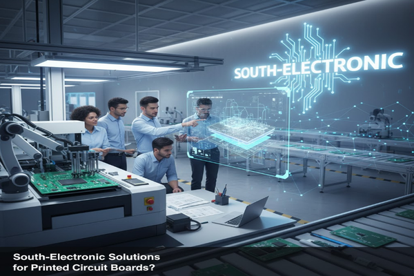
When I've needed specific solutions for my projects, I've learned that a good partner makes all the difference. It's not just about getting a board made; it's about getting the right board, quickly and efficiently. south-electronic positions itself as a comprehensive provider, aiming to support customers at every stage of the PCB lifecycle.
How south-electronic Addresses PCB Needs
- Full-Spectrum Manufacturing Capabilities:
- Prototyping: Offers quick-turn PCB prototypes, essential for early design verification and iteration. This reduces development cycles and costs.
- Mass Production: Provides scalable manufacturing for high-volume orders, ensuring consistent quality and cost-effectiveness.
- Specialized Boards: Caters to unique requirements such as flexible PCBs[^10], rigid-flex PCBs, high-frequency boards, and heavy copper boards for specific applications.
- Design and Engineering Support:
- DFM (Design for Manufacturability): Provides expert feedback during the design phase to optimize boards for efficient and cost-effective production, minimizing potential issues.
- DFA (Design for Assembly): Assists in optimizing the layout for automated component placement and soldering, improving yield rates.
- Component Sourcing: Leverages an established supply chain network to procure quality components, mitigating supply risks.
- Quality Assurance and Testing:
- Rigorous Inspection: Implements various inspection methods including Automated Optical Inspection (AOI) and X-ray inspection for internal layers.
- Electrical Testing: Conducts comprehensive electrical tests (e.g., flying probe, bed of nails) to guarantee circuit integrity.
- Certifications: Adheres to industry standards (e.g., ISO, UL, RoHS) to ensure compliance and reliability.
- Supply Chain Management:
- Global Sourcing: Utilizes a global network to source materials and components, ensuring competitive pricing and availability.
- Logistics: Manages the entire logistics process, from raw material procurement to final product delivery, streamlining the customer experience.
Conclusion
PCBs are the invisible force powering our electronic world. Understanding their creation, the teams behind them, and their vast applications reveals their critical importance in every aspect of modern technology.
[^1]: Learn about the various electronic components that work together on PCBs to create functional devices. [^2]: Discover how conductive tracks are essential for connecting components on a PCB. [^3]: Understand the importance of copper sheets in creating the pathways for electrical signals. [^4]: Explore the different substrate materials that provide the foundation for PCBs. [^5]: Find out how CAD software aids engineers in designing intricate PCB layouts. [^6]: Learn about Gerber files and their role as blueprints in the PCB manufacturing process. [^7]: Discover how PCBs are integral to the functionality of modern automotive systems. [^8]: Learn about the importance of PCBs in ensuring the reliability of medical equipment. [^9]: Understand how effective supply chain management impacts PCB production and delivery. [^10]: Discover the unique characteristics and uses of flexible PCBs in various industries.

