
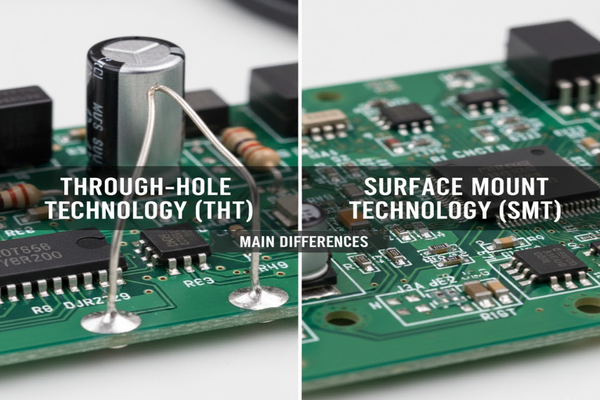
Are you confused by circuit board jargon? Do terms like "through-hole" and "surface mount" leave you scratching your head? You're not alone, and I’m here to clear things up.
Through-hole technology involves inserting component leads into drilled holes on a PCB, while surface mount technology[^1] solders components directly onto the board's surface. These fundamental differences impact board size, manufacturing, and component density[^2] significantly.

Understanding these differences is crucial for anyone involved in electronics, from hobbyists to professional engineers. Let's dive deeper into what makes each technology unique and why it matters for your projects.
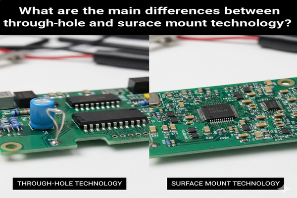
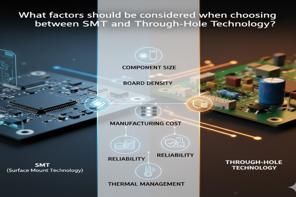
What factors should be considered when choosing between SMT and through-hole technology?
Struggling to decide between SMT and through-hole for your next project? Making the wrong choice can lead to headaches, cost overruns, and missed deadlines. I know, I've been there!
When choosing between SMT and through-hole, I consider factors like component size[^3], board density, manufacturing cost[^4], reliability[^5], and thermal management[^6]. Each technology has unique strengths that make it suitable for different applications.

When I'm deciding between SMT and through-hole, I always look at several key areas. First, component size is a big one. Through-hole components are generally larger, which means they take up more space on the board. SMT components are tiny, allowing for much denser designs. This leads directly to board density; if I need a compact product, SMT is usually the way to go. Manufacturing cost is another critical factor. While SMT requires specialized automated equipment[^7], it can be more cost-effective for high-volume production[^8] due to speed and efficiency. Through-hole often involves more manual assembly, which can increase labor costs for large runs. Reliability is also on my mind. Through-hole components offer a very strong physical connection, which can be beneficial in high-vibration environments. SMT, while excellent, relies more on the solder joint for mechanical strength. Finally, thermal management plays a role. Larger through-hole components can sometimes dissipate heat more effectively due to their size, but advanced SMT designs can also handle significant thermal loads with proper planning.
| Factor | Surface Mount Technology (SMT) | Through-Hole Technology (THT) |
|---|---|---|
| Component Size | Much smaller, compact designs possible | Larger, takes up more board space |
| Board Density | High component density, components on both sides | Lower component density, components on one side |
| Manufacturing | Automated pick-and-place, reflow soldering, high volume | Manual assembly, wave soldering, lower volume |
| Cost | Lower for high volume, higher initial equipment cost | Higher for high volume (labor), lower initial equipment cost |
| Reliability | Good electrical performance, less mechanical strength | Stronger mechanical connection, good for high-stress areas |
| Thermal Mgmt. | Requires careful design for heat dissipation | Larger components can offer better heat dissipation |
What are the advantages of surface mount technology?
Are you still using older, bulkier circuit designs? Feeling limited by the size and complexity of your electronic products? I've found that embracing SMT can unlock incredible possibilities.
Surface mount technology offers numerous advantages, including increased component density for smaller boards, higher manufacturing efficiency through automation, improved electrical performance, and lower costs for high-volume production[^8], making it ideal for modern electronics.
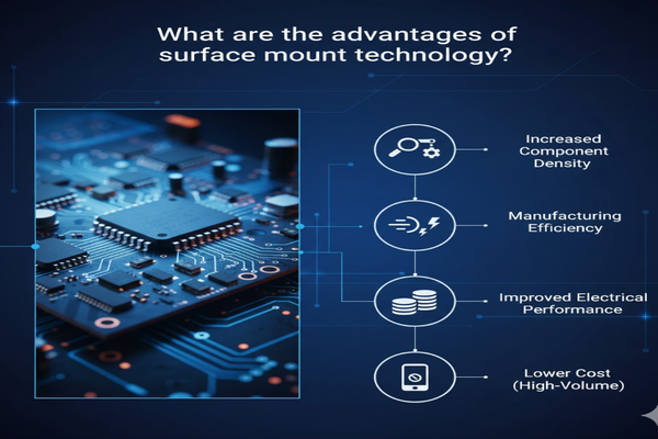
I've personally seen the benefits of SMT transform product designs. One of the biggest advantages is the sheer increase in component density. Because SMT components are so small and can be placed on both sides of a PCB, I can pack more functionality into a much smaller footprint. This directly leads to more compact and lighter electronic devices, which is a huge selling point in today's market. Manufacturing efficiency is another major plus. With automated pick-and-place machines, SMT assembly is incredibly fast and precise. This means I can produce boards at a much higher volume and with greater consistency than manual through-hole methods. I also appreciate the improved electrical performance. Shorter lead times and reduced parasitic inductance and capacitance mean better signal integrity and higher operating frequencies, which is crucial for high-speed applications. Finally, for large production runs, the overall cost per unit tends to be lower with SMT once the initial setup costs are absorbed. This combination of size, speed, performance, and cost makes SMT a powerful tool in my design arsenal.
| Advantage | Description | My Personal Impact |
|---|---|---|
| Increased Density | SMT components are tiny, allowing more components per unit area and placement on both sides of the board. This results in smaller, lighter, and more portable devices. | I once had a project where the client needed a device to fit into an incredibly small enclosure. Without SMT, it would have been impossible to meet their size requirements. I loved seeing how much functionality I could fit into such a tight space. |
| Higher Automation | SMT assembly is highly automated using robotic pick-and-place machines and reflow ovens. This leads to faster production speeds, reduced labor costs, and greater consistency in manufacturing. | When I moved from manual soldering to automated SMT, the production speed was astonishing. What took hours now took minutes, and the consistency across boards was a game-changer for quality control. |
| Improved Performance | Shorter lead lengths in SMT components reduce parasitic inductance and capacitance, leading to better high-frequency performance, reduced noise, and improved signal integrity. This is vital for high-speed digital and RF circuits. | I remember troubleshooting a high-frequency circuit with through-hole components where signal integrity was a nightmare. Switching to SMT immediately cleaned up the signals, and the circuit performed as expected. It was a real eye-opener for me. |
| Lower Cost (Volume) | While initial setup for SMT can be expensive, the per-unit cost for high-volume production[^8] is typically lower due to faster assembly, reduced material usage (less PCB material), and fewer errors compared to manual through-hole assembly. | For a large production run, I calculated that SMT cut our manufacturing cost[^4]s by nearly 30% compared to if we had used through-hole. That savings allowed us to be much more competitive in the market. |
What are the disadvantages of surface mount technology?
Considering SMT for your next design but worried about potential pitfalls? While SMT offers many benefits, it's not without its challenges. I've learned these lessons the hard way, so you don't have to.
Surface mount technology does have disadvantages, including increased vulnerability to mechanical stress, difficulty with manual prototyping or repair due to small component sizes, higher initial equipment investment, and challenges with thermal management in dense layouts.
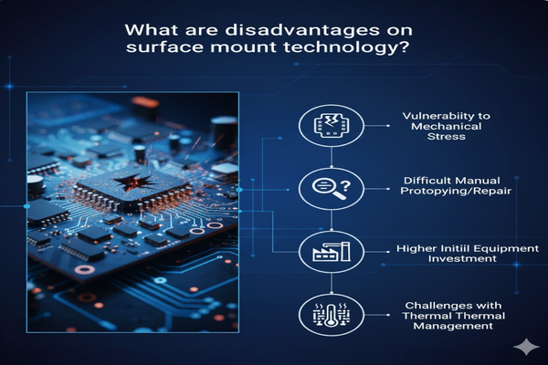
Even with all its advantages, I've run into my share of issues with SMT. One significant disadvantage is the increased vulnerability to mechanical stress. Because SMT components are soldered directly to the surface, they rely entirely on the solder joint for both electrical and mechanical connection[^9]. This means they can be more susceptible to damage from vibration or bending compared to through-hole components, which have leads passing through the board for extra support. Another hurdle for me has been the difficulty with manual prototyping and repair. Those tiny components are great for density but a nightmare to work with by hand! Reworking a faulty SMT component often requires specialized tools and a steady hand, which makes quick fixes or initial prototyping more challenging. The initial equipment investment can also be substantial. While high-volume production sees cost savings, getting started with SMT requires purchasing expensive pick-and-place machines and reflow ovens, which can be a barrier for smaller operations. Finally, I've had to pay very close attention to thermal management in dense SMT layouts. Packing so many components into a small space can lead to localized hotspots, and heat dissipation needs careful design consideration to prevent component failure.
| Disadvantage | Description | My Personal Learning |
|---|---|---|
| Mechanical Vulnerability | SMT components rely solely on solder joints for mechanical connection, making them less robust against physical stress, vibration, and bending compared to through-hole components with leads anchored through the board. | I once designed a device for a high-vibration environment using SMT. We experienced unexpected failures until I realized the solder joints weren't strong enough. I learned to add mechanical bracing or consider specific SMT packages better suited for stress. |
| Difficult Prototyping/Repair | The small size of SMT components makes manual soldering, prototyping, and rework extremely challenging, often requiring specialized tools like microscopes, fine-tipped soldering irons, and hot air stations. | Early in my career, I tried to hand-solder a complex SMT prototype. It was a nightmare of misplaced components and solder bridges. I quickly learned the value of professional assembly services even for prototypes, or at least investing in the right tools. |
| Higher Initial Investment | Setting up an SMT production line requires a significant capital investment in automated equipment such as pick-and-place machines, reflow ovens, screen printers, and inspection systems, which can be prohibitive for small businesses. | When my team first considered moving to SMT in-house, the upfront cost for equipment was a huge barrier. We had to carefully weigh the long-term volume benefits against that initial outlay. It was a big financial decision that required strong justification. |
| Thermal Management Issues | The high component density in SMT can lead to localized heat buildup. Effective thermal management becomes critical, requiring careful PCB layout, heat sinks, and sometimes active cooling solutions to prevent overheating and ensure component longevity. | I designed a power-intensive SMT board once and underestimated the thermal output. The device would occasionally shut down due to overheating. I had to go back and add thermal vias, copper pours, and even a small heat sink in a redesign, adding to development time. |
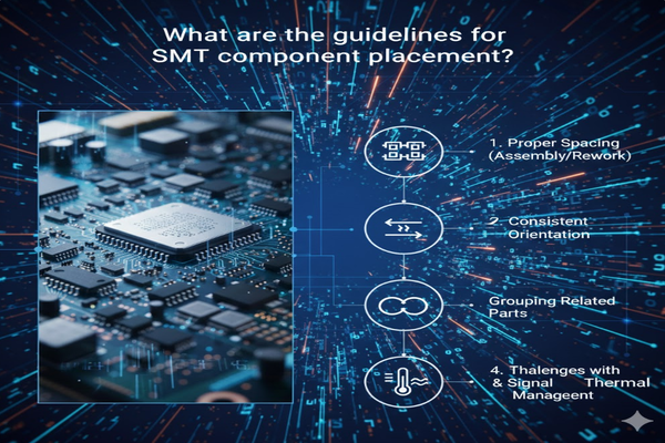
What are the guidelines for SMT component placement?
Are your SMT designs prone to errors or manufacturing issues? Poor component placement can lead to costly rework and performance problems. I’ve refined my placement strategies over many projects. Effective SMT component placement follows guidelines such as maintaining proper spacing for assembly and rework, orienting components consistently, grouping related parts, considering thermal dissipation, and planning for signal integrity to ensure manufacturability and optimal performance.  When I’m laying out an SMT board, I always follow a set of guidelines to avoid headaches later on. First, maintaining proper spacing between components is absolutely critical. This isn't just for electrical clearance; it's also essential for the pick-and-place machine to accurately place parts and for rework if something goes wrong. If components are too close, the machine might struggle, or I won't be able to get a soldering iron in for repair. Second, I always orient components consistently. For example, all similar polarized components (like diodes or electrolytic capacitors) should have their positive or negative ends facing the same direction. This reduces errors during assembly and makes visual inspection much easier. Third, I group related components together. Keeping a microcontroller close to its crystal oscillator and bypass capacitors minimizes trace lengths, which improves signal integrity and reduces noise. Fourth, I actively consider thermal dissipation. High-power components generate heat, so I place them where they can dissipate heat effectively, perhaps with copper pours or away from heat-sensitive parts. Lastly, I meticulously plan for signal integrity. Critical traces should be kept short and direct, avoiding unnecessary bends or vias, especially for high-speed signals, to ensure the circuit performs as intended.
| Guideline | Description | My Personal Application |
|---|---|---|
| Maintain Proper Spacing | Ensure sufficient clearance between components, especially between larger and smaller parts, to allow for automated placement, soldering, inspection, and potential rework without interference or solder bridging. Adhere to manufacturing design rules. | I learned this the hard way on an early design where I packed components too tightly. The pick-and-place machine had trouble, and hand rework was almost impossible. Now, I always leave a buffer, especially around ICs and connectors. |
| Consistent Orientation | Place polarized components (diodes, capacitors, ICs) with consistent orientation. This simplifies assembly, reduces the chance of incorrect placement, and makes visual inspection much faster and more reliable. | For me, consistent orientation is a non-negotiable. I remember one batch of boards where a technician accidentally rotated a polarized capacitor on a few boards because the silkscreen marking was unclear, leading to malfunctions. Now I'm extra careful about clear, consistent markings. |
| Group Related Components | Position components that work together (e.g., an IC and its bypass capacitors, or a connector and its associated filtering components) close to each other. This minimizes trace lengths, reduces noise, and improves signal integrity. | I always group power supply components or a microcontroller with its support circuitry. It makes the schematic easier to follow on the board, and I've found it significantly reduces noise issues in sensitive circuits. |
| Consider Thermal Dissipation | Place high-power or heat-generating components (e.g., power regulators, MOSFETs) in areas with good airflow or with dedicated thermal pads/vias. Avoid placing heat-sensitive components directly adjacent to heat sources. | I had a power converter IC that kept failing on a prototype. After some investigation, I realized it was too close to another heat-generating component with no thermal relief. Redesigning its placement and adding a dedicated copper pour solved the issue. |
| Plan for Signal Integrity | Route high-speed traces short and direct, avoiding sharp turns (use 45-degree angles), unnecessary vias, and routing under noisy components. Isolate sensitive analog signals from noisy digital signals to prevent interference. | On a high-speed data acquisition board, I initially routed traces haphazardly. I got corrupted data. I then learned to use controlled impedance traces, avoid unnecessary vias, and shield sensitive lines. The data became crystal clear after that. |
Conclusion
Understanding the differences between through-hole and surface mount technologies, their pros, cons, and placement guidelines, is essential for informed electronics design.
[^1]: Explore the benefits of surface mount technology to enhance your electronic designs and manufacturing efficiency. [^2]: Discover the importance of component density for optimizing space and functionality in circuit boards. [^3]: Learn how component size influences design choices and overall product performance. [^4]: Understanding manufacturing costs can help you make informed decisions for your electronic projects. [^5]: Explore reliability factors to choose the best technology for your electronic applications. [^6]: Effective thermal management is crucial for ensuring the longevity and performance of electronic devices. [^7]: Discover the automated equipment that enhances efficiency and precision in surface mount technology. [^8]: Understanding high-volume production can help you optimize costs and efficiency in manufacturing. [^9]: Learn why mechanical connections are vital for the durability and reliability of electronic components.

