
Ever sent PCB files to a factory, only to discover missing layers after production? File confusion causes delays. Let me walk you through must-have documents for smooth manufacturing.
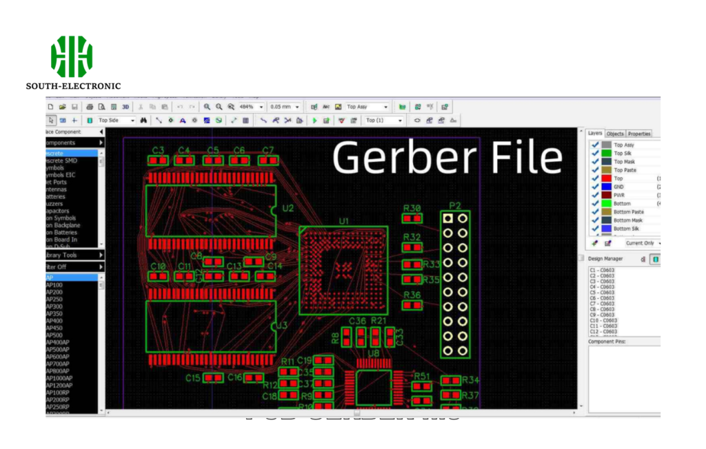
For PCB printing, submit GERBER files[^1] (copper/solder mask layers), BOM list[^2] (components), XY coordinates (placement data), and original PCB design files. Double-check file versions and approve material specs with your manufacturer upfront to avoid costly rework. Full documentation ensures first-time success.
Getting the files right is half the battle. Below I’ll break down prototyping fundamentals and explain how each document impacts your project’s timeline, quality, and budget.
Introduction to PCB Prototyping
Rushing to mass production without testing is like baking a cake without tasting the batter. Prototypes catch design flaws early.
PCB prototyping[^3] creates functional samples to verify circuit performance, component placement, and manufacturability. It identifies errors in schematics, routing, or material selection before full-scale production, saving up to 70% in potential redesign costs.
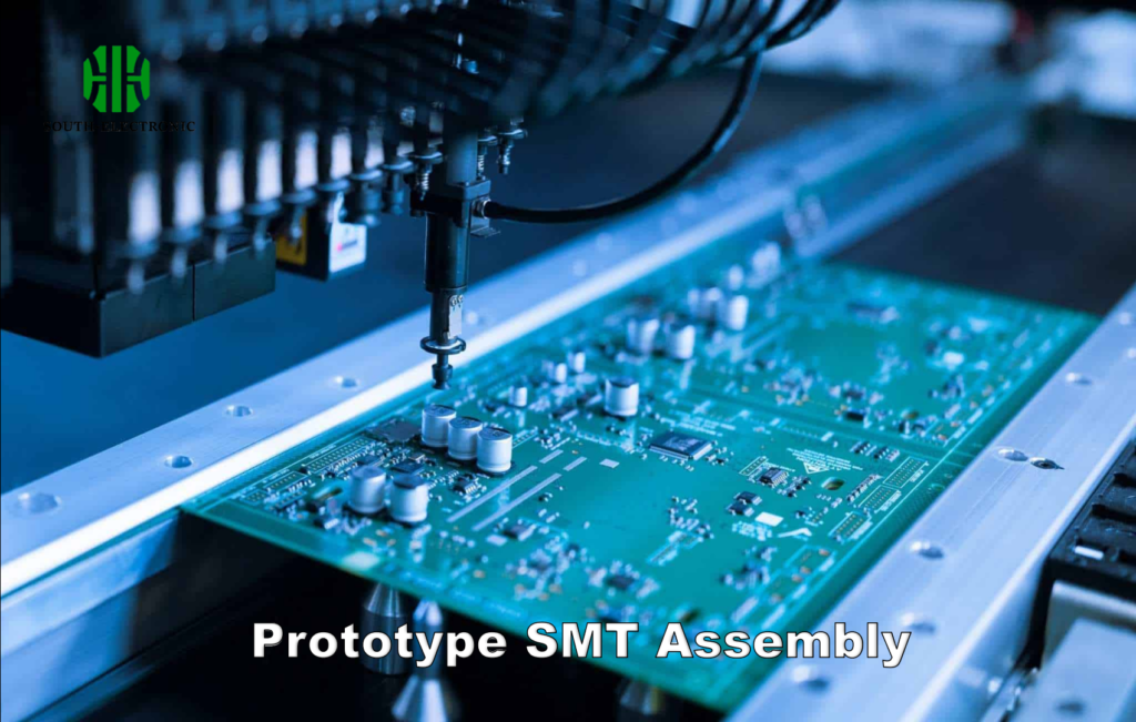)
Three Stages of Effective Prototyping
| Stage | Purpose | Key Activities |
|---|---|---|
| Design Proof | Validate basic functionality | Run simulations, check DRC |
| Alpha Build | Test real-world performance | Assemble 5-10 boards, run EMI/stress tests |
| Pre-Production | Finalize manufacturing process | Verify panelization, confirm yield rates |
Start with 2-layer boards for simple designs, allocating 2-3 weeks per iteration. Budget 20% extra for unexpected component swaps – I once burned 15 boards due to incorrect resistor footprints!
Files Required for PCB Prototyping
Missing the assembly drawing? Your PCB becomes a $200 paperweight. Learn the 4 non-negotiable files every manufacturer demands.
Submit GERBER (RS-274X format), BOM (Excel/CSV with MPNs), XY coordinates (Centroid format), and native design files (Altium/KiCad). Confirm layer stackup and impedance requirements in a separate tech pack to prevent misunderstandings.
)
File Requirements Checklist
| Document | Format | Critical Data Points | Common Pitfalls |
|---|---|---|---|
| GERBER | .GBR (ZIP) | Layer count, drill holes, solder mask | Missing soldermask_TOP layer |
| BOM | Excel | Manufacturer part numbers, quantities | Using internal codes instead of MPNs |
| XY Coordinates[^4] | .CSV | Component rotation, placement side | Millimeter/inch unit mismatch |
| PCB Original | .PcbDoc/.SchDoc | Netlist, design rules | Outdated revision (v1 vs v2) |
Always zip files with clear naming: "ProjectName_Rev2_Gerber.zip". Last month, a client sent "final_final_new.zip" containing 2019 files – their production got delayed by 11 days.
PCB Prototyping Precautions: How to Avoid Costly Surprises?
Assuming your factory "knows what you want" is prototyping suicide. Two engineers once ordered FR-4[^1] boards but got ceramic substrates – communication matters.
Confirm board material (FR-4/Rogers), surface finish[^2] (HASL/ENIG), copper weight (1oz/2oz), and tolerances (±0.2mm) in writing. Request DFM reports[^3] and pre-production samples to catch process errors early.
)
Material/Treatment Tradeoffs
| Parameter | Low-Cost Option | High-Reliability Option | When to Choose |
|---|---|---|---|
| Surface Finish | HASL (Lead-Free) | ENIG (Gold Plating) | High-density components |
| Dielectric | FR-4 (Standard) | Rogers 4350B | High-frequency (>5GHz) |
| Copper Thickness | 1oz (35µm) | 2oz (70µm) | High-current power circuits |
| Silkscreen | White Epoxy | LPI Legend | Fine-pitch labeling |
Demand coupons (test patterns) on panel edges. One client rejected 500 boards due to unverified impedance – their 50Ω traces measured 47Ω without test points.
Conclusion
Submit complete GERBER, BOM, XY, and design files, detailing materials and specs. Prototype iteratively, verify all documents match revisions, and never skip factory DFM checks. Preparation prevents PCB headaches.
[^1]: Understanding GERBER files is crucial for ensuring accurate PCB production and avoiding costly mistakes. Explore this link to learn more.
[^2]: A BOM list is essential for component management in PCB projects. Discover its importance and how to create one effectively.
[^3]: PCB prototyping helps identify design flaws early, saving time and costs. Learn more about its benefits and processes here.
[^4]: XY coordinates are vital for component placement in PCBs. Learn how to effectively use them in your designs.
[^5]: Understanding the properties of FR-4 can help you make informed decisions for your PCB projects.
[^6]: Exploring surface finishes will enhance your knowledge of PCB reliability and performance.
[^7]: Learning about DFM reports can help you avoid costly mistakes in your PCB production process.

