

Ever get confused by acronyms like SMD? Whether you’re soldering circuits or chatting tech, misunderstandings waste time. Let me clear this up fast.
SMD primarily means Surface-Mount Device – components soldered onto PCBs. However, context matters: it can be Sega Mega Drive (gaming), Standardized Mean Difference (stats), or Severe and Multiple Disadvantages (social work).
Now that we’ve decoded SMD, let’s explore its most common application: stencil-based PCB manufacturing. The real magic happens when we apply this knowledge practically.
What are the two types of stencils?
Struggling with messy solder paste application? Choosing wrong stencils causes uneven deposits. Understanding types eliminates this headache.
Electronics uses two stencil types: framed (permanent metal-bound) and frameless (disposable membrane). Framed suits mass production; frameless works best for quick prototypes and DIY projects.
Why type selection impacts results
Your stencil framework determines durability and cost. Framed stencils use tensioned stainless steel for 50k+ prints but cost $150-$500. Frameless options like polyester sheets cost under $10 but tear after 2-5 uses.
Here’s how they compare:
| Feature | Framed Stencil | Frameless Stencil |
|---|---|---|
| Cost | $100+ | $5-$20 |
| Durability | 10,000-100,000 prints | 2-10 prints |
| Setup | Requires holder/jig | Tape-mounted |
| Best for | Production lines | DIY/hobbyist projects |
Always match stencil type to project scale. For hobbyists, frameless + smd stencil jig saves money. Manufacturers need framed versions for smd stencil soldering consistency. Remember thickness too – frameless often uses thinner 0.1mm material versus standard 0.15mm framed smd stencil thickness.
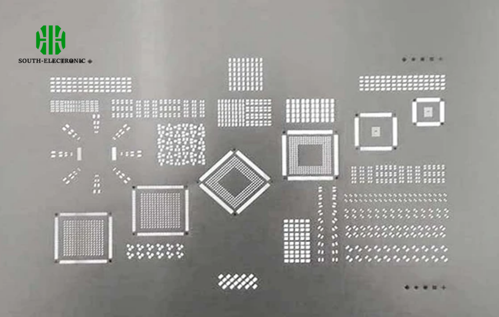
What key design rules apply to SMD stencil apertures?
Frustrated by paste clogs or weak joints? Bad aperture design causes messy bleeding. Follow critical guidelines to prevent defects.
Apertures need 1.5 area ratio (hole area divided by wall area) for proper paste release. Aspect ratios over 1.5 prevent clogging. Always make aperture walls trapezoidal with 2°-5° taper.
Design principles explained
Aperture geometry directly impacts solder volume. Small IC pads risk bridging with oversize openings, while large components suffer weak connections with undersized apertures. Your smt stencil printer relies on these rules:
- Round apertures help release paste cleanly
- Rectangular openings need rounded corners (radius ≥ paste particle size)
- Component spacing determines wall thickness – 0.3mm minimum spacing requires 0.125mm walls
Critical ratios:
- Area ratio = (length × width) / [2(length+width)thickness] → must exceed 0.66
- Aspect ratio = width / thickness → should exceed 1.5
Ignore these and you’ll waste paste and time cleaning stencils. When ordering from smd stencil pcbway, supply exact ratio calculations. Good design enables reliable smd stencil soldering without clogging.
What affects SMD stencil costs?
Shocked by price quotes that vary 500%? Hidden cost factors trip up beginners. Knowing these saves your budget.
Five factors dominate pricing: material grade (stainless steel vs nickel), thickness tolerance (±0.001mm premium), size (over 37x47cm costs 30% more), frame requirements, and special features like step-stencils.

Breaking down the variables
Cost drivers fall into material, labor, and complexity categories. Stainless steel costs $0.50/cm², while electroformed nickel triples that price. Large panels exceeding standard sizes add laser cutting fees.
| Cost Factor | Low-Cost Option | Premium Option | Price Impact |
|---|---|---|---|
| Material | 301 Stainless Steel | Nickel alloy | +200-300% |
| Thickness | ±0.005mm tolerance | ±0.001mm tolerance | +80% |
| Size | Under 30x30cm | Over 37x47cm | +40% |
| Features | Basic cutouts | Multi-level step-downs | +150% |
Pro tip: For smd stencil diy, use polyimide film costing $8/sheet instead of steel ($80+). But production needs proper smd stencil framework. Always confirm smd stencil thickness specs – 0.1mm saves paste but costs more per sheet. Service like smd stencil pcbway bulk orders cuts per-unit prices.
Conclusion
SMD mainly means Surface-Mount Devices, where stencils are vital. Remember: choose framed/frameless wisely, follow aperture ratios, and control costs through material choices.

