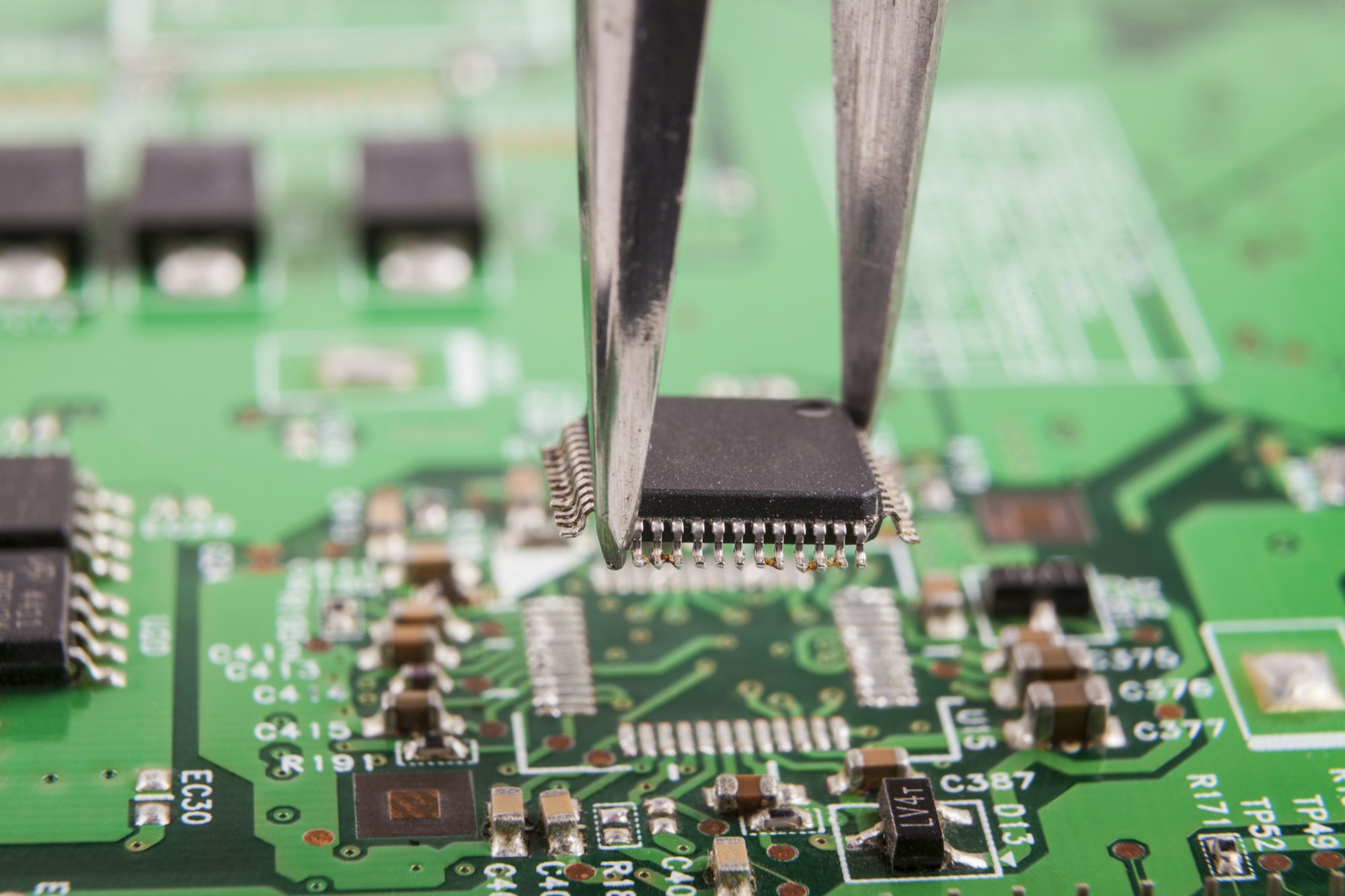
Having trouble with complex electronics? Ever wonder how small devices pack so much power? Multilayer PCBs are the unsung heroes making it all possible.
A Multilayer PCB is a circuit board with three or more conductive layers laminated together with insulating material. This design allows for higher component density and more complex circuitry, crucial for modern electronic devices.
I remember when I first stumbled upon the term "multilayer PCB." It sounded really technical, but I soon learned it's a fundamental part of almost every advanced electronic device we use daily. Once you get what they are, you will see how they shape our tech world. Let's dig in and simplify this vital technology.
How Would You Define a Multilayer PCB?
Are your electronic designs hitting a wall with space or performance? Multilayer PCBs offer a solution by stacking circuit layers, making smaller, more powerful devices possible.
A Multilayer PCB integrates multiple layers of copper traces and insulating substrates, creating a compact and highly functional circuit board. This layered construction boosts performance and reduces electromagnetic interference.

When I think about multilayer PCBs, I picture a tiny skyscraper for electronics. Instead of components living on one floor, they spread out across several levels, connected by tiny elevators called vias. This allows for incredible packing density and performance. Here's a breakdown of their key features:
Layer Stack-up and Insulating Layers
A multilayer PCB is built like a sandwich. You have alternating layers of copper, which carry electrical signals, and insulating materials, which keep those signals from shorting out.
- Copper Layers: These are where the traces, pads, and planes are located. They carry current and signals.
- Prepreg: This is a fiberglass material impregnated with resin, which acts as the glue and insulation between core layers during lamination.
- Core: This is a rigid fiberglass laminate, usually copper-clad on both sides, providing structural integrity. Imagine building a highway system: you can have multiple levels of roads, and the space between them is crucial to prevent collisions.
Interconnection Vias
How do signals travel between these layers? That is where vias come in.
- Through-hole Vias: These go all the way through the board, connecting all layers.
- Blind Vias: These connect an outer layer to one or more inner layers but do not go all the way through.
- Buried Vias: These connect only inner layers and are not visible from the outside. These vias are like the stairwells or elevators in our skyscraper analogy, allowing movement between floors.
Ground and Power Layers
Many multilayer PCBs include dedicated ground and power planes.
- Ground Planes: These provide a stable reference voltage and help reduce noise.
- Power Planes: These distribute power efficiently to all components. Having dedicated planes helps manage current flow and minimize electromagnetic interference (EMI), leading to a cleaner signal.
Higher Density and Complexity
The main reason for using multilayer PCBs is to fit more functionality into a smaller space. By spreading circuits vertically, designers can create incredibly complex and powerful devices. This increased density also allows for better signal integrity and controlled impedance.
- Component Placement: More surface area for components.
- Trace Routing: More paths for signals to travel without crossing or interfering.
How are Multilayer PCBs Manufactured?
Are you curious about how these intricate boards are made? The process for multilayer PCBs involves several precise steps, ensuring high functionality and reliability.
Manufacturing multilayer PCBs requires meticulous steps: designing, fabricating inner layers, laminating them together, drilling connections, plating holes, adding solder masks, and rigorous testing for quality.

I always find it fascinating to see how something so complex is put together with such precision. Making a multilayer PCB is not just one step; it is a whole journey with many important checkpoints. Each stage needs to be perfect to make sure the final board works correctly. Let me walk you through the key steps involved:
Design and Layout
Every PCB starts with a detailed design. Engineers use specialized software to create the circuit diagram and then arrange the components and traces on each layer. This includes defining the layer stack-up, deciding on via types, and planning for signal integrity.
- CAD Software: Tools like Altium Designer or Eagle are used for this.
- Stack-up Definition: Deciding the order and material of each layer.
Inner Layer Fabrication
The copper layers that will be inside the board are made first. This involves cleaning the copper-clad laminate, applying a photoresist, exposing it to UV light with a circuit pattern, and then etching away unwanted copper.
- Cleaning: Removes dirt and oils.
- Photoresist Application: A light-sensitive film.
- Exposure: Transfers the circuit image.
- Etching: Removes copper not protected by photoresist. After etching, these individual inner layers are inspected for defects.
Stack-up and Lamination
This is where the magic of "multilayer" happens. The prepared inner layers, along with prepreg and copper foil (for outer layers), are stacked precisely. This stack is then subjected to high pressure and heat in a lamination press. The heat causes the resin in the prepreg to flow and cure, bonding all the layers together into a single, solid board.
- Layer Alignment: Crucial for proper connections.
- Heat and Pressure: Cures the resin and fuses layers.
Drilling
Once laminated, thousands of tiny holes are drilled through the board. These holes will become the vias that connect different layers. Precise computer-controlled drills are used to ensure accuracy.
- CNC Drilling Machines: Automated for high precision.
- Tooling Holes: Used for alignment in later steps.
Hole Plating and Outer Layer Imaging
After drilling, the inside surfaces of the holes are coated with a thin layer of copper. This process, called electroplating, creates electrical pathways through the vias. Next, the outer copper layers are imaged and etched, similar to the inner layers, to create the final circuit patterns.
- Electroless Copper Deposition: Initializes plating.
- Electrolytic Copper Plating: Builds up copper thickness in holes.
- Outer Layer Etching: Defines the external traces.
Solder Mask and Silkscreen
A solder mask, usually green, is applied to the board to protect the copper traces from oxidation and prevent solder bridges during assembly. Finally, a silkscreen layer adds component outlines, labels, and logos, aiding in assembly and troubleshooting.
- Solder Mask Application: Protects circuits.
- Silkscreen Printing: Adds visual information.
Surface Treatment, Testing, and Quality Control
The exposed copper pads (where components will be soldered) receive a surface finish, such as ENIG (Electroless Nickel Immersion Gold) or HASL (Hot Air Solder Leveling), to improve solderability and prevent oxidation. The finished PCBs undergo rigorous electrical testing (e.g., flying probe or bed of nails) to check for shorts, opens, and proper connectivity. Visual inspections also ensure quality.
- Surface Finish: Ensures good soldering.
- Electrical Testing: Verifies circuit integrity.
- Final Inspection: Checks for cosmetic and functional defects.
What are the Advantages and Disadvantages of Multilayer PCBs?
Considering a multilayer PCB for your next project? Understanding their pros and cons is key to making the best choice for performance and cost.
Multilayer PCBs offer high density and improved performance, but they come with increased manufacturing complexity and higher costs. Weighing these factors helps determine if they are right for your needs.
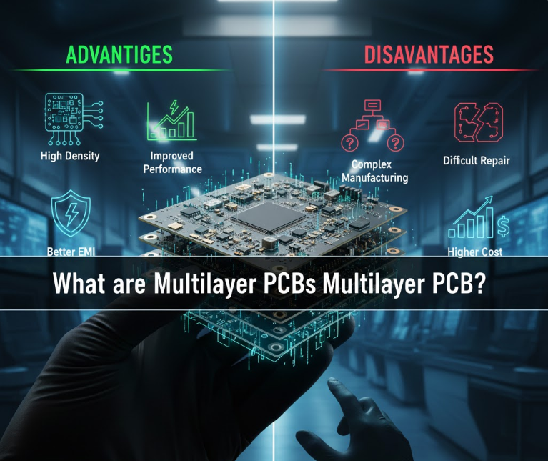
When I'm deciding on a PCB type for a new design, I always think about what is important: performance, size, or cost? Multilayer PCBs bring some amazing benefits, but they also have drawbacks you need to know about. It is all about finding the right balance for your project. Let us look at both sides.
Advantages
Multilayer PCBs really shine when you need a lot of power in a small package.
- Increased Density: This is the big one. By stacking layers, you can fit many more components and traces into a smaller area. This means more functionality in a compact device. Imagine going from a sprawling ranch house to a multi-story apartment building.
- Improved Performance: Shorter trace lengths between components lead to faster signal propagation and reduced signal degradation. Dedicated ground and power planes also help reduce noise and electromagnetic interference (EMI), making for a more stable and reliable circuit.
- Enhanced Electrical Characteristics: Controlled impedance can be more easily achieved, which is vital for high-speed signals. This helps maintain signal integrity and prevent reflections.
- Greater Flexibility (with flexible multilayer): While most are rigid, flexible multilayer PCBs offer unique advantages for applications requiring bending or conforming to irregular shapes.
Disadvantages
However, these benefits do not come without a price.
- Higher Cost: More layers mean more materials, more complex manufacturing steps, and more testing, all of which drive up the cost per board. This is usually the first thing I consider when budgeting a project.
- Complex Manufacturing: The fabrication process is much more intricate than for single or double-sided boards. This complexity can lead to longer lead times and a higher chance of manufacturing defects if not done by an experienced manufacturer.
- Debugging Challenges: With many layers, tracing signals and identifying faults can be much harder. If a component is on an inner layer or a via has an issue, it is not as easy to fix as on a simple board. Specialized equipment is often needed for diagnostics.
- Increased Weight and Thickness: While denser, a board with many layers can be thicker and heavier than a simpler board, though this is often offset by the overall size reduction of the final product.
What are the Applications of Multilayer PCBs?
Wondering where multilayer PCBs are used? From the smartphone in your pocket to complex medical devices, these boards are everywhere, powering advanced technology.
Multilayer PCBs are found in high-tech devices requiring compact, powerful electronics. They are essential for mobile phones, medical equipment, aerospace systems, and high-performance computing due to their density and reliability.
I often look around and realize just how much we rely on devices powered by multilayer PCBs. They are the hidden engines behind so much of our modern world. When a device needs to be small, fast, and reliable, a multilayer PCB is often the go-to solution. Let us explore some of the places where these boards truly shine.
Consumer Electronics
Almost every portable electronic device we use daily relies on multilayer PCBs.
- Smartphones and Tablets: These devices demand incredible processing power and functionality in a very thin form factor. Multilayer PCBs allow for the high component density needed.
- Smartwatches and Wearables: Their tiny size and advanced features are only possible because of compact multilayer circuitry.
- Laptops: Modern laptops are powerful and thin, thanks to the space-saving benefits of multilayer boards. These are applications where space is at an absolute premium, and performance cannot be compromised.
Medical Devices
Reliability and precision are critical in medical applications, and multilayer PCBs deliver both.
- Implantable Devices: Pacemakers and defibrillators use multilayer PCBs for their small size and robustness.
- Diagnostic Equipment: MRI machines, CT scanners, and ultrasound systems benefit from the high signal integrity and noise reduction offered by multilayer designs.
- Monitoring Devices: Equipment that monitors vital signs often uses these boards to ensure accurate and consistent readings. The demand for high reliability and consistent performance makes multilayer PCBs ideal for saving lives and improving health.
Automotive Industry
Modern cars are essentially computers on wheels, and multilayer PCBs are fundamental to their advanced systems.
- Engine Control Units (ECUs): These complex systems manage engine performance and emissions.
- Infotainment Systems: From navigation to media playback, these systems require compact and powerful electronics.
- Advanced Driver-Assistance Systems (ADAS): Features like adaptive cruise control, lane-keeping assist, and parking assist rely on high-density PCBs for sensor processing. As vehicles become more automated and connected, the need for sophisticated electronics, powered by multilayer PCBs, continues to grow.
Aerospace and Defense
In applications where failure is not an option and conditions are extreme, multilayer PCBs provide the necessary reliability and performance.
- Avionics: Flight control systems, navigation, and communication equipment in aircraft and spacecraft.
- Radar Systems: High-frequency signals and complex processing require excellent signal integrity.
- Missile Guidance Systems: These systems demand compact, robust, and highly reliable electronics. The ability of these boards to withstand harsh environments and provide unwavering performance is paramount in these sectors.
Telecommunications
The infrastructure that keeps us connected worldwide relies heavily on multilayer PCBs.
- Servers and Routers: Data centers and network hardware utilize these boards for high-speed data processing and communication.
- Base Stations: Cellular towers and other communication infrastructure require reliable, high-density circuitry to manage vast amounts of data traffic.
- Fiber Optic Equipment: Managing high-bandwidth optical signals demands precision and minimal interference.
Multilayer PCBs are truly everywhere, acting as the backbone for almost all advanced electronic technology.
Conclusion
Multilayer PCBs stack conductive layers for density and performance. They are vital for compact, high-tech devices, despite higher costs and manufacturing complexity.

