

Are you curious about the silent workhorse inside almost every electronic device you own? Printed Circuit Boards power our modern world, but many people don't fully understand what they are.
A Printed Circuit Board (PCB)[^1] is a flat, insulated surface with conductive pathways[^2], typically copper, that connects electronic components. It provides mechanical support and electrical connections for parts like chips, resistors, and connectors, forming a complete circuit.
I remember the first time I opened an old radio; the green board with all the tiny parts seemed like magic. Today, PCBs are far more complex and vital. Let's peel back the layers and discover the fascinating world of these essential components.
What are the different types of PCBs?
Ever wonder if all those green boards are the same? They aren't! Different electronic needs call for different PCB structures.
PCBs come in several forms, each designed for specific applications. The main types include single-sided, double-sided, multi-layer, rigid, flexible, and rigid-flex PCBs[^3], offering varying levels of complexity and adaptability.
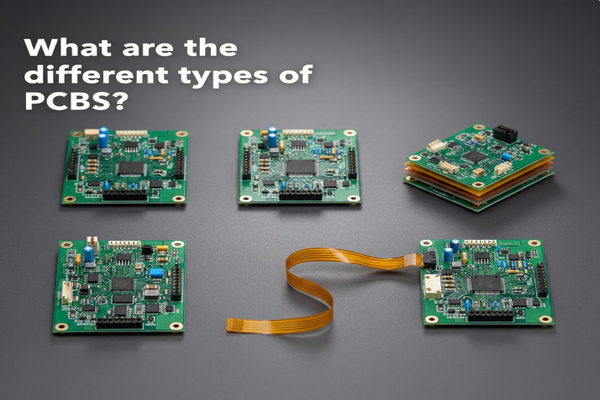
When I started learning about electronics, I thought a circuit board was just a circuit board. But as I dove deeper, I found that the choice of PCB type is a critical engineering decision, impacting everything from performance to cost.
Single-Sided PCBs
These boards have components and traces on only one side. They are simple and cost-effective, ideal for basic electronics.
- Structure: One layer of conductive material on an insulating substrate.
- Applications: Simple devices like calculators, LED lighting, power supplies.
Double-Sided PCBs
These PCBs have conductive traces on both sides, with holes (vias) connecting the layers. They allow for more complex circuits.
- Structure: Two layers of conductive material separated by an insulating layer.
- Applications: Industrial controls, vending machines, automotive dashboards.
Multi-Layer PCBs
These boards consist of three or more conductive layers stacked together. They enable very dense and complex circuit designs.
- Structure: Multiple layers of traces separated by dielectric materials, interconnected by vias.
- Applications: Smartphones, computers, servers, medical equipment.
Flexible PCBs
"Flex circuits" are made on a flexible plastic substrate, allowing them to bend and conform to various shapes.
- Structure: Conductive traces on a flexible polymer film.
- Applications: Wearable devices, cameras, automotive sensors.
Rigid-Flex PCBs
These combine elements of both rigid and flexible boards, offering the best of both worlds.
- Structure: Rigid PCB sections connected by flexible PCB sections.
- Applications: Medical implants, aerospace systems, high-end consumer electronics[^4].
| PCB Type | Complexity | Cost | Flexibility | Common Uses |
|---|---|---|---|---|
| Single-Sided | Low | Low | No | Calculators, simple power supplies |
| Double-Sided | Medium | Medium | No | Vending machines, industrial controls |
| Multi-Layer | High | High | No | Smartphones, computers, data servers |
| Flexible | Medium | Medium-High | Yes | Wearables, cameras, automotive sensors |
| Rigid-Flex | Very High | Very High | Partial | Medical implants, aerospace, military |
What are the applications of PCBs in various industries?
Have you ever stopped to think about how many devices in your daily life rely on PCBs? The answer might surprise you.
PCBs are the foundational components for nearly all electronic devices, driving innovation across countless industries. From consumer electronics and automotive systems to medical devices[^5] and aerospace, their applications are incredibly diverse and essential for modern technology.
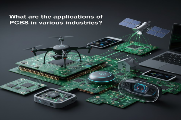
I often tell people that if you can plug it in or put a battery in it, there's probably a PCB inside. My own journey into understanding electronics made me realize just how pervasive these boards are. Their impact spans almost every sector you can imagine.
Consumer Electronics
This is where most of us interact with PCBs daily. Think about the devices we use for communication, entertainment, and daily tasks.
- Smartphones & Tablets: Compact, multi-layer PCBs[^6] enable powerful processing and connectivity.
- Computers & Laptops: Complex motherboards, graphics cards, and other internal components.
- Televisions & Audio Equipment: Control circuits for display, sound processing, and connectivity.
- Wearable Devices: Flexible and rigid-flex PCBs[^3] fit into small, ergonomic designs.
Automotive Industry
Modern cars are essentially computers on wheels, and PCBs are critical for their advanced features and safety systems.
- Engine Control Units (ECUs): Manage engine performance, fuel efficiency, and emissions.
- Infotainment Systems: Navigation, communication, and entertainment modules.
- Advanced Driver-Assistance Systems (ADAS): Sensors, cameras, and radar systems for safety features.
- LED Lighting Systems: Control boards for efficient and dynamic vehicle lighting.
Medical Devices
Reliability and precision are paramount in medical applications, making high-quality PCBs indispensable.
- Diagnostic Equipment: MRI machines, CT scanners, ultrasound devices.
- Implantable Devices: Pacemakers, cochlear implants use miniature, often rigid-flex, PCBs.
- Monitoring Systems: Patient monitors, blood glucose meters, and other portable health devices.
Industrial Applications
PCBs are the backbone of automation and control systems that power factories and infrastructure.
- Industrial Control Systems: PLCs (Programmable Logic Controllers) and motor control drives.
- Robotics: Control boards for robotic arms and automated machinery.
- Power Distribution: Circuit breakers, power converters, and energy management systems.
Aerospace and Defense
In these fields, extreme reliability, high performance, and resistance to harsh environments are critical.
- Avionics: Flight control systems, navigation equipment, communication arrays.
- Satellite Systems: On-board computers, communication transceivers.
- Military Hardware: Radar systems, missile guidance, ruggedized communication devices.
| Industry | Key PCB Applications | Examples of Devices |
|---|---|---|
| Consumer Electronics | Processing, connectivity, display control | Smartphones, Laptops, Smartwatches |
| Automotive | Engine management, safety, infotainment | ECUs, ADAS, Dashboard displays |
| Medical | Diagnostics, monitoring, therapeutic devices | MRI machines, Pacemakers, Glucose meters |
| Industrial | Automation, control, power management | PLCs, Robotic controllers, Motor drives |
| Aerospace & Defense | Flight control, navigation, communication, weaponry | Avionics, Satellites, Radar systems |
How are PCBs manufactured?
Ever thought about the journey a simple circuit board takes from design to finished product? It’s a fascinating, multi-step process!
PCB manufacturing[^7] is a complex, multi-stage process involving design, material selection, etching, drilling, plating, and component assembly. Each step requires precision and specialized equipment to transform a conceptual circuit into a functional electronic board.
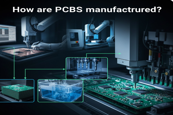
I used to think PCBs just appeared, fully formed. But seeing the manufacturing process firsthand or even in videos reveals the incredible engineering involved. It’s a testament to human ingenuity, turning raw materials into the brains of our devices.
Design and Layout
The first step is translating the circuit diagram into a physical layout. This is done using specialized software.
- Schematic Capture: Designing the electronic circuit diagram.
- PCB Layout: Arranging components and drawing conductive traces on a virtual board.
- Gerber Files: Outputting design data files used by manufacturers for each layer.
Material Preparation
The base material, typically fiberglass (FR-4), is chosen for its insulating properties and durability.
- Copper Cladding: A layer of copper is bonded to one or both sides of the substrate.
- Cutting: The large panels are cut into sizes suitable for processing.
Etching and Imaging
This process defines the conductive pathways on the copper layers.
- Inner Layer Imaging (for multi-layer PCBs): Applying a photoresist material, exposing it to UV light through a film, and developing it to create the circuit pattern.
- Etching: Removing unwanted copper from the board, leaving only the desired circuit traces.
- Lamination (for multi-layer PCBs): Stacking multiple etched layers with prepreg (insulating material) and pressing them together under heat to form a solid board.
- Drilling: Precision drilling machines create holes (vias) for component leads and inter-layer connections.
Plating
This makes the drilled holes conductive and reinforces the copper traces.
- Electroless Copper Deposition: A thin layer of copper is chemically deposited onto the hole walls.
- Electroplating: A thicker layer of copper is electroplated onto the holes and exposed traces.
Outer Layer Imaging and Etching
Similar to inner layer imaging, but for the final outer layers, often including solder mask application[^8].
- Solder Mask Application: A protective layer (usually green) is applied to prevent solder bridges during assembly.
- Silkscreen Printing: Component designators, logos, and other markings are printed onto the board.
Final Finishing
These steps prepare the PCB for component assembly.
- Surface Finish: Applying a metallic coating (e.g., HASL, ENIG) to protect exposed copper and ensure solderability.
- Electrical Testing: Testing for shorts, opens, and other electrical defects to ensure functionality.
- Routing: Cutting the large panel into individual PCBs.
| Stage | Description | Key Technologies Involved |
|---|---|---|
| Design | Creating circuit schematics and board layouts | CAD software (e.g., Altium Designer, Eagle) |
| Imaging & Etching | Defining circuit patterns on copper | Photolithography, Chemical etching baths |
| Drilling | Creating holes for components and interconnections | CNC drilling machines, Laser drills |
| Plating | Making holes conductive, reinforcing traces | Electroless plating, Electroplating, Chemical deposition |
| Solder Mask & Silkscreen | Protecting traces, adding markings | Screen printing, Photoimaging, Inkjet printing |
| Testing & Finishing | Verifying functionality, preparing for assembly | Flying probe testers, Optical inspection, Routing machines |
Conclusion
PCBs are the unsung heroes of electronics, enabling everything from simple calculators to complex medical devices. Understanding their types, applications, and manufacturing reveals their incredible importance in our tech-driven world.
[^1]: Explore this link to understand the fundamental role of PCBs in electronics. [^2]: Learn about the importance of conductive pathways in connecting electronic components. [^3]: Learn how rigid-flex PCBs combine rigidity and flexibility for advanced uses. [^4]: Explore the critical role of PCBs in everyday consumer devices. [^5]: Understand the importance of PCBs in ensuring reliability in medical technology. [^6]: Understand the advantages of multi-layer PCBs for complex electronic designs. [^7]: Learn about the intricate process of PCB manufacturing from design to assembly. [^8]: Explore how solder masks protect PCBs during assembly.

