
Are you struggling with complex circuit boards and their tiny components? It can be frustrating when you do not understand how these parts work together.
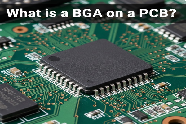
A Ball Grid Array (BGA)[^1] on a PCB is a chip package. It connects to the board using solder balls underneath. This design allows for more connections in a small space, making devices smaller and more powerful.
I remember the first time I saw a BGA. I was amazed at how many connections it could have in such a small area. It made me wonder about the different types and why engineers choose them. Let's explore these questions together.
How many types of BGA are there?
Ever feel overwhelmed by all the different electronic component types? It is easy to get lost in the jargon and wonder which one is right for your project.
There are many types of BGA packages, each with unique features. Common types include standard BGA, fine-pitch BGA (FBGA)[^2], micro BGA (µBGA)[^3], and chip-scale package (CSP). These variations offer different sizes and connection densities for various applications.

Let us dive deeper into these BGA types. Each one offers benefits for specific engineering needs. Understanding these differences helps in choosing the right package.
Standard BGA
Standard BGAs are common. They have solder balls spaced further apart. This makes them easier to assemble and inspect. They are good for applications where space is not extremely tight. My friend used one in a simple control board. He found it reliable and relatively easy to work with.
Fine-Pitch BGA (FBGA)
FBGAs have smaller solder balls. The spacing between them is also smaller. This allows for more connections in the same area. They are used in devices needing high pin counts. Think of memory modules or complex processors. The manufacturing process for FBGAs is more precise.
Micro BGA (µBGA)
µBGAs are even smaller. They use tiny solder balls. These are ideal for very compact devices. Mobile phones and wearable tech often use µBGAs. The small size helps reduce the overall device footprint. However, they are harder to work with due to their miniature scale.
Chip-Scale Package (CSP)[^4]
A CSP is a type of BGA. Its size is close to the actual chip size. This means the package is almost as small as the silicon die itself. CSPs are excellent for miniaturization. They are common in smartphones and digital cameras.
| BGA Type | Key Feature | Common Use |
|---|---|---|
| Standard BGA | Wider ball pitch | General electronics |
| Fine-Pitch BGA | Smaller ball pitch | Memory, processors |
| Micro BGA | Tiny balls, small size | Mobile devices |
| CSP | Package size near chip size | Smartphones, cameras |
What is the difference between BGA and LGA?
Do you ever get confused between BGA and LGA, wondering which one is which? It is common to mix them up when looking at circuit board components.
The main difference between BGA and LGA is where the connection pins are. BGA uses solder balls on the package that connect to pads on the PCB. LGA uses flat pads on the package that connect to pins on the socket on the PCB.

Let's look closer at how BGA and LGA connect to the PCB. This will show us why each one is useful. I had to learn this difference when I was designing my first custom PC.
Ball Grid Array (BGA)[^1]
BGA packages have solder balls directly on the bottom. These balls melt during reflow soldering. They form a permanent connection to the PCB pads. This creates a very strong electrical and mechanical bond. Once soldered, removing a BGA requires specialized tools. This makes it less suitable for user-replaceable components. My experience taught me that BGA soldering needs precision.
Land Grid Array (LGA)
LGA packages have flat lands or pads on the bottom. These pads mate with spring-loaded pins inside a socket on the PCB. The chip is placed into the socket and a retention mechanism holds it in place. This makes LGA ideal for components that might need upgrading or replacing, like computer CPUs. You can easily remove and insert an LGA chip without soldering.
Comparison
The choice between BGA and LGA depends on the application. BGAs offer excellent electrical performance. This is because of their short connection paths. They are great for high-frequency signals. LGAs offer flexibility. They let users swap out parts. This is useful for upgrades or repairs. For example, CPUs in desktop computers are almost always LGA. This lets you upgrade your processor easily.
| Feature | BGA | LGA |
|---|---|---|
| Connection Type | Solder balls on package | Flat pads on package |
| PCB Connection | Solder pads on PCB | Socket with pins on PCB |
| Removability | Difficult to remove | Easy to remove/replace |
| Applications | Permanent components, high-density | User-upgradable components (CPUs) |
| Soldering | Reflow soldering | Socket mechanical connection |
Why is BGA used?
Have you ever wondered why engineers choose BGA over other packaging types? It seems like a complex way to connect a chip, but there are strong reasons behind it.
BGA is used for several key reasons: high pin count[^5], better electrical performance[^6], improved thermal management[^7], and smaller form factor. This packaging allows for more connections in a compact space, which is critical for modern, powerful devices.

Let's break down these reasons. When I first learned about BGA, I realized it solved many problems older packages faced. This knowledge really helped me understand modern electronics better.
High Pin Count
As integrated circuits become more complex, they need more input/output (I/O) connections. Traditional packages, like Quad Flat Packages (QFP), have leads on the sides. As pin count increases, these leads become very fine and fragile. They also take up a lot of board space. BGA uses the entire bottom surface for connections. This allows for hundreds or even thousands of I/Os in a small area. This is a huge advantage for microprocessors and complex FPGAs.
Better Electrical Performance
The short solder balls in a BGA provide excellent electrical performance. Shorter connections mean less inductance and capacitance. This is important for high-speed signals. It reduces signal noise and improves signal integrity. For me, this meant faster data transfer in the devices I was working on.
Improved Thermal Management
Heat is a major issue in high-performance chips. BGA packages often have a large thermal path through the solder balls to the PCB. The PCB acts as a heatsink, helping dissipate heat. Some BGAs also have a thermal pad in the center. This pad connects directly to the PCB ground plane. This design helps keep the chip cool, extending its lifespan and performance.
Smaller Form Factor
The ability to pack more I/O into a smaller footprint is vital. Modern electronics are always shrinking. BGA helps achieve this miniaturization. It frees up valuable space on the PCB for other components. This is why you see BGAs in almost all small, powerful devices like smartphones and laptops. My personal project always struggles with space, so BGA is a lifesaver.
| Advantage | Explanation | Impact |
|---|---|---|
| High Pin Count | Uses entire bottom for I/O | More complex chips in small space |
| Electrical Performance | Short connections, low inductance | Faster, cleaner signals |
| Thermal Management | Heat path through balls/pad | Cooler chip, longer life |
| Smaller Form Factor | Compact packaging | Miniaturized devices |
How does BGA work?
Have you ever wondered about the magic inside a BGA package? It seems like a simple block, but its internal workings are quite clever.
A BGA works by connecting an integrated circuit chip to a substrate within the package. This substrate then has an array of tiny solder balls on its bottom surface. During assembly, these solder balls melt and form electrical connections to corresponding pads on the printed circuit board.

Let's walk through the steps of how a BGA works. Understanding this process helped me appreciate the engineering involved in every circuit board.
Internal Structure
Inside a BGA package, the actual silicon chip (the die) is mounted onto a substrate. This substrate is usually made of a laminate material. The chip connects to this substrate using very fine wires (wire bonding) or flip-chip technology. The substrate has traces that route these chip connections to the underside of the package.
Solder Balls
On the bottom of the substrate, a precise grid of solder balls is attached. These balls are made of a specific solder alloy. Each ball corresponds to a specific electrical connection needed by the chip. When the BGA package is placed on the PCB, these balls align with pads on the board.
Reflow Soldering
The key to a BGA connection is reflow soldering[^8]. The BGA package is placed on the PCB. Then, the entire assembly goes into a reflow oven. The oven heats the assembly to a controlled temperature. This melts the solder balls. Surface tension causes the molten solder to pull the package into perfect alignment. As the assembly cools, the solder solidifies. This forms a strong electrical and mechanical bond between the BGA and the PCB. I once messed up a reflow profile and the connections were bad. It taught me the importance of precise temperature control.
Inspection
After soldering, it is hard to visually inspect BGA connections. This is because the solder joints are hidden under the package. Special techniques are used. These include X-ray inspection[^9]. X-rays can "see through" the package to check the solder joint quality. This ensures all connections are good.
| Step | Description | Key Mechanism |
|---|---|---|
| 1. Chip Mounting | Chip connected to internal substrate | Wire bonding/Flip-chip |
| 2. Solder Ball Array | Solder balls attached to substrate bottom | Pre-formed solder spheres |
| 3. Placement on PCB | BGA aligned to PCB pads | Pick-and-place machine |
| 4. Reflow Soldering | Heat melts solder, forms connections | Surface tension, controlled heating/cooling |
| 5. Inspection | Checking hidden solder joints | X-ray inspection |
Conclusion
BGAs are crucial for modern electronics, enabling high-density connections and better performance. They are essential for smaller, more powerful devices we use daily.
[^1]: Understanding BGA is essential for grasping modern electronics design and its advantages. [^2]: Explore FBGA to see how it enables high-density connections in advanced electronics. [^3]: Discover the significance of µBGA in compact devices like smartphones and wearables. [^4]: CSP is crucial for miniaturization; learn how it impacts device design. [^5]: High pin count is vital for complex chips; explore its implications in design. [^6]: Learn how BGA enhances signal integrity and reduces noise in high-speed applications. [^7]: Explore thermal management to understand how it prolongs chip lifespan and performance. [^8]: Reflow soldering is critical for BGA connections; learn about its process and importance. [^9]: X-ray inspection ensures quality in BGA solder joints; discover its significance.

