

Tired of burnt components and failed prototypes? PCB simulation acts as your virtual lab, exposing hidden design flaws before you pay factory costs. Ignore it, and risk costly delays.
PCB simulation[^1] creates digital models to test circuit behavior under real-world conditions like heat, signal interference, and power surges. It prevents costly physical prototyping errors by identifying issues early in the design phase.
But how exactly does this virtual testing work? And why do even experienced engineers rely on it? Let’s demystify the process step by step.
What Exactly Happens in a PCB Simulation?
Imagine X-ray vision for your circuit board. Simulation software dissects your design layer by layer, predicting failures most designers miss.
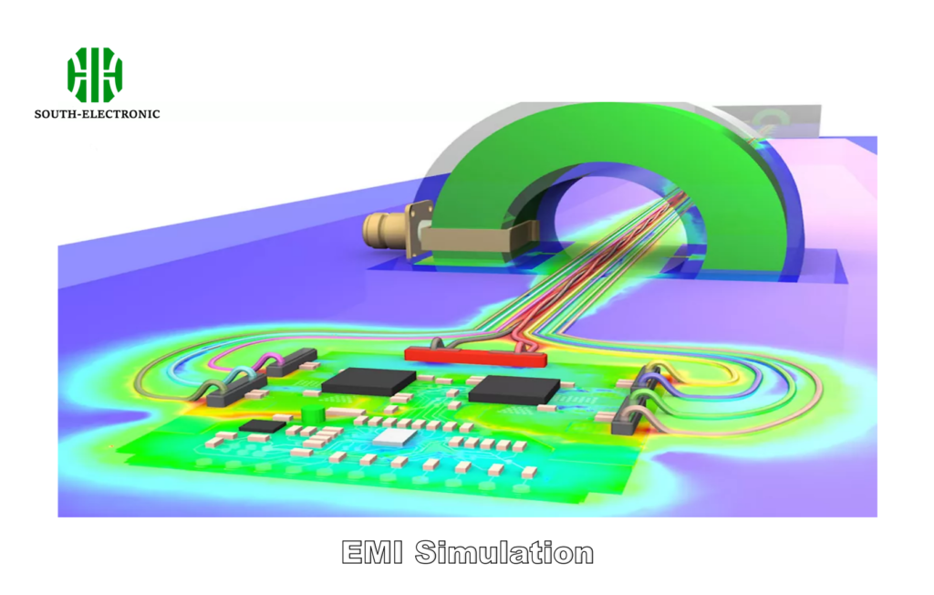
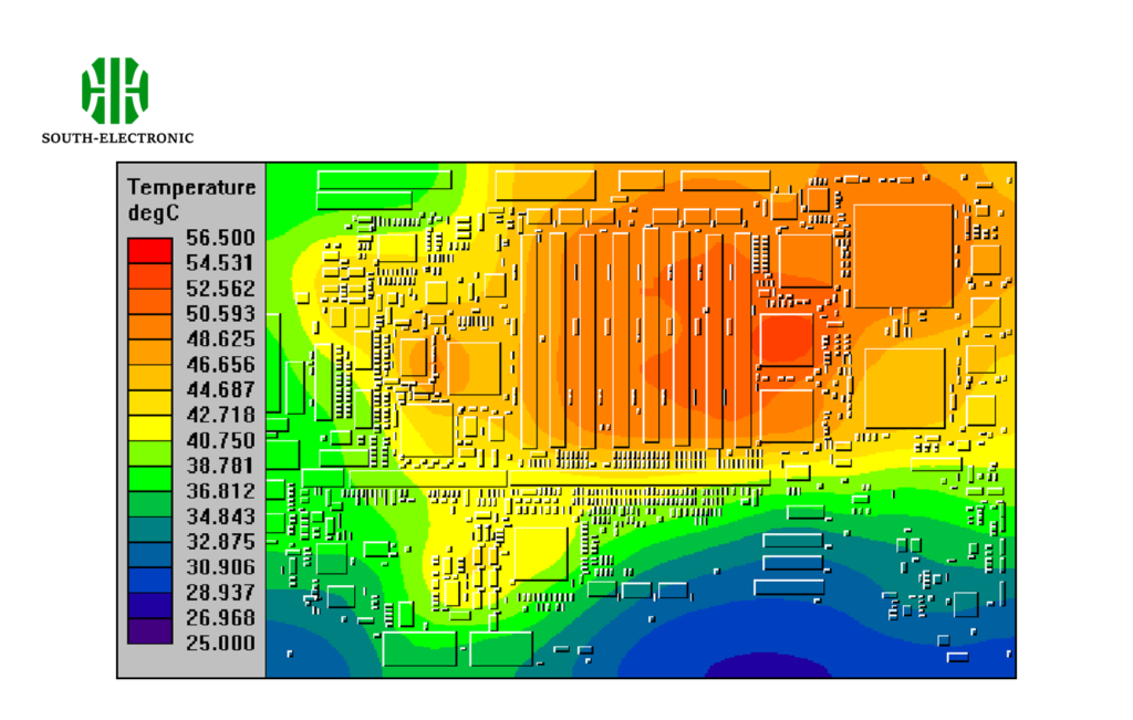
PCB simulation analyzes electrical performance, thermal behavior[^2], and signal integrity[^3] through mathematical models. It replicates scenarios like sudden voltage spikes or prolonged heat exposure to verify component safety margins.
)
The 3-Stage Simulation Process
- Model Creation
- Import CAD designs
- Define material properties (copper thickness, substrate type)
- Parameter Setup
- Input voltage ranges
- Set temperature thresholds
- Assign signal frequencies
- Analysis & Validation
- Run EMI/EMC checks
- Monitor heat dissipation patterns
| Stage | Tools Used | Common Issues Detected |
|---|---|---|
| Model Creation | Altium Designer, KiCad | Incorrect trace spacing |
| Parameter Setup | ANSYS Icepak, COMSOL | Overvoltage risks |
| Validation | Cadence Sigrity | Signal crosstalk |
I once simulated a motor controller board that passed all bench tests. The software revealed a hidden voltage drop during cold starts – a flaw that could’ve caused field failures. This preemptive fix saved $28k in potential recalls.
Why Can’t You Afford to Skip PCB Simulations?
One client called it "financial Russian roulette." Without simulations, you’re gambling with production budgets and brand reputation.
Skipping simulations risks undetected design flaws that cause field failures, recalls, and safety hazards. A single thermal oversight can melt $5k worth of components during stress testing.
)
Cost Comparison: Simulation vs Physical Prototyping
| Factor | Simulation | Physical Test |
|---|---|---|
| Time per iteration | 2-4 hours | 2-3 weeks |
| Cost per iteration | $150 (software) | $1,200 (materials+labor) |
| Defect detection rate[^4] | 92% (all major issues) | 67% (visible issues only) |
Real-world example: A medical device company found mounting screw currents causing ECG interference via simulation. Physical tests missed this because it only appeared with specific body contact conditions. Fixing post-production would’ve required retooling 15 injection molds.
Which Software is Best for Circuit Simulation?
With 47+ tools available, choosing feels overwhelming. Your ideal pick depends on three key factors: budget, complexity, and team skills.
For beginners, free tools like LTSpice handle basic analog simulations. Enterprise teams use ANSYS or Cadence for multi-physics analysis. Check compatibility with your existing CAD software to avoid file conversion nightmares.
)
Simulation Software Breakdown
| Tool | Best For | Learning Curve | Cost Range |
|---|---|---|---|
| LTSpice | Analog circuits | Low | Free |
| Altium Nexus | Signal integrity | Medium | $8k/year |
| ANSYS HFSS | RF & microwave | High | $25k+/year |
| COMSOL | Thermal analysis | Medium-High | $15k+/year |
Case study: A drone manufacturer switched from KiCad to ANSYS after realizing their 5 GHz video transmitter caused gyroscope noise. The advanced tool modeled electromagnetic interference they couldn’t test physically until flight crashes occurred.
What Hidden Challenges Do Beginners Often Face?
New users often crash into the "simulation cliff[^5]" – models that look perfect but give garbage results. Why? Missing real-world variables.
Common pitfalls include ignoring component tolerances, improper ground plane modeling, and underestimating environmental factors like humidity. Always cross-verify simulation results with manual calculations for critical parameters.
)
Beginner Mistake Handbook
| Error Type | Why It Happens | Solution |
|---|---|---|
| Over-idealized components | Using default lib. models | Import manufacturer SPICE files |
| Incorrect mesh density | Coarse mesh saves compute time | Use adaptive mesh refinement |
| DC-only validation | Missing AC/transient analysis | Test all operational modes |
Example: A new engineer simulated a power supply only at 25°C room temp. Real-world testing failed when ambient reached 40°C – capacitors derated beyond simulation assumptions. Now we always run thermal sweeps[^6] from -10°C to 85°C.
Conclusion
PCB simulation acts as your design safety net, catching costly errors early. From component selection to environmental resilience, virtual testing bridges the gap between theoretical designs and real-world reliability.
[^1]: Explore this link to understand the fundamentals of PCB simulation and its importance in circuit design, ensuring you avoid costly mistakes.
[^2]: Learn about the impact of thermal behavior on PCB design to enhance your understanding of heat management in electronics.
[^3]: Discover the significance of signal integrity in PCB design to ensure reliable performance and avoid communication issues in circuits.
[^4]: Understanding defect detection rates can help you make informed decisions about testing methods, ensuring higher quality in your products.
[^5]: Understanding the simulation cliff can help you avoid common pitfalls in PCB design and improve your simulation accuracy.
[^6]: Learning about thermal sweeps can enhance your understanding of how temperature variations affect component performance in real-world scenarios.

