

Struggling with complex BGA routing? Many engineers face this challenge. Without proper fanout, your high-performance designs can hit a roadblock.
BGA fanout[^1] is how we route electrical signals from a BGA chip's tiny solder balls to the rest of the PCB. It's crucial for dense circuit boards, ensuring all connections are made without short circuits.
Understanding BGA fanout is not just about connecting points; it's about optimizing your entire board's performance and manufacturability. Let's dig deeper into what makes a successful fanout strategy.
What are important considerations for BGA fanout design?
Facing tight spaces and complex BGA pinouts? Poor planning can lead to signal integrity issues and manufacturing headaches.
Key considerations for BGA fanout design include ball pitch[^2], pin count[^3], PCB layer stack-up[^4], via technology[^5], and signal integrity[^6]. These elements dictate the routing strategy and overall board complexity.
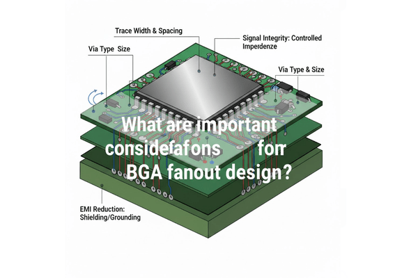
When I approach a BGA fanout, I start by looking at the specific BGA package. The ball pitch is fundamental; a finer pitch (like 0.4mm) means smaller traces and vias. Pin count, especially for high-density BGAs with hundreds or thousands of pins, directly impacts the required number of PCB layers. If you have many pins, you'll need more layers to escape all the signals. I always consider the PCB layer stack-up early on, as this helps decide if I can use standard vias or if I need more advanced options like microvias or via-in-pad. Signal integrity is another big one. High-speed signals need careful routing to avoid crosstalk and impedance mismatches. I ask myself: What are the critical signals? Do they need differential routing? What are the power and ground requirements? These questions guide my initial setup. I also look at manufacturing capabilities, because a design that's hard to build is a bad design.
| Consideration | Impact on Design | Why it Matters |
|---|---|---|
| Ball Pitch | Determines trace width and via size. | Finer pitch needs smaller features, higher complexity. |
| Pin Count | Dictates required PCB layers. | More pins = more layers to route signals. |
| Via Technology | Influences routing density and cost. | Microvias allow denser routing but cost more. |
| Signal Integrity | Affects high-speed performance. | Poor design leads to data loss and system instability. |
| Manufacturing | Ensures board can be built reliably. | Design must align with fab house capabilities. |
How do you create an optimized design?
Want to avoid design revisions and save costs? An optimized BGA fanout is crucial. Without it, you risk delays and signal issues.
Creating an optimized BGA fanout involves selecting appropriate via types, employing proper escape routing patterns[^7], managing layer transitions efficiently, and using simulation tools for validation.
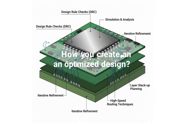
My approach to optimization always begins with understanding the signal types. Power and ground pins need robust connections, often with multiple vias per pad. For high-speed signals, I prioritize direct, short routes and try to minimize via transitions. I use different fanout patterns depending on the BGA pitch and pin count. For example, a dog bone pattern works well for larger pitches, while via-in-pad or staggered microvias are essential for fine-pitch BGAs. I always try to route the critical signals on the innermost layers first to shield them. Layer transitions are tricky. Each via adds inductance and capacitance, so I try to limit them for critical signals. I use a hierarchical approach: first, fan out the outer rows, then work my way inward. This helps me manage the density. I also leverage design rule checks (DRC)[^8] aggressively and, for very complex designs, I use signal integrity (SI) simulation tools. These tools help me predict how signals will behave before I even send the board to manufacturing. It's about finding the right balance between manufacturability, performance, and cost.
| Optimization Strategy | Benefit | Example Technique |
|---|---|---|
| Via Selection | Maximizes routing density, minimizes space. | Via-in-pad for fine pitch, through-hole for power. |
| Routing Patterns | Ensures efficient signal escape. | Dog bone, staggered via, channel routing. |
| Layer Management | Reduces signal degradation, simplifies routing. | Prioritize critical signals on inner layers. |
| Simulation & DRC | Validates design, prevents costly errors. | SI analysis, automated design rule checks. |
| Power/Ground Planes | Provides stable references, reduces noise. | Dedicated planes, multiple stitching vias. |
What is the added value of an optimized BGA fanout?
Tired of frustrating design failures and costly re-spins? An optimized BGA fanout is your secret weapon. Without it, you're inviting problems.
An optimized BGA fanout offers improved signal integrity, reduced EMI, lower manufacturing costs, faster design cycles, and enhanced overall product reliability, providing a significant competitive advantage.
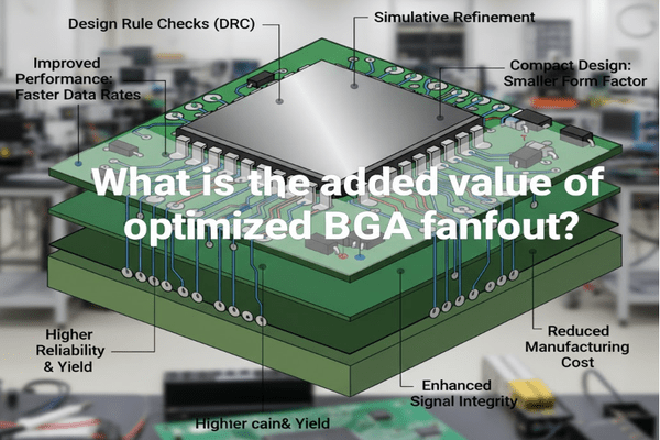
I've seen firsthand how an optimized BGA fanout can transform a project. The most immediate benefit is enhanced signal integrity. When traces are routed correctly, with proper impedance control and minimal discontinuities, high-speed signals transmit cleanly. This prevents data errors and ensures the device operates at its intended performance level. Reduced electromagnetic interference (EMI) is another huge plus. By carefully planning ground planes and shielding, I can minimize unwanted radiation, which is crucial for meeting regulatory compliance. From a cost perspective, an efficient fanout can reduce the number of PCB layers required or allow for less expensive via technologies. This directly impacts manufacturing costs. Furthermore, a well-planned fanout accelerates the design cycle. Less time spent on manual routing and fewer design revisions mean a faster time to market. Ultimately, it leads to a more reliable product. A board that's designed right from the start is less prone to field failures, improving customer satisfaction and reducing warranty claims. It's an investment that pays off across the entire product lifecycle.
| Value Proposition | Direct Impact | Long-Term Benefit |
|---|---|---|
| Signal Integrity | Clean signal transmission. | Reliable device operation, higher performance. |
| Reduced EMI | Minimized unwanted radiation. | Regulatory compliance, improved system stability. |
| Lower Cost | Fewer PCB layers, simpler manufacturing. | Reduced production expenses, better profit margins. |
| Faster Design Cycle | Quicker routing, fewer revisions. | Shorter time to market, competitive advantage. |
| Product Reliability | Fewer field failures, consistent performance. | Enhanced brand reputation, increased customer loyalty. |
Conclusion
Optimized BGA fanout is essential for modern electronics. It ensures robust signal integrity, reduces costs, and speeds up development, leading to reliable, high-performance products.
[^1]: Understanding BGA fanout is crucial for optimizing PCB designs and ensuring reliable connections. [^2]: Ball pitch is a key factor in determining trace width and routing complexity in PCB layouts. [^3]: Pin count directly influences the number of PCB layers needed, impacting design complexity. [^4]: The layer stack-up is essential for determining routing strategies and overall board performance. [^5]: Understanding via technology helps in optimizing routing density and managing costs effectively. [^6]: Signal integrity is critical for ensuring reliable data transmission and preventing system instability. [^7]: Escape routing patterns are vital for efficiently connecting BGA pins to the PCB without signal loss. [^8]: DRC helps prevent design errors, ensuring that the PCB meets all necessary specifications.


