
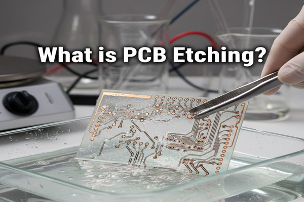
Are you curious about how circuit boards get their intricate patterns? Frustrated with unreliable electronics? Understanding PCB etching is key to reliable devices.
PCB etching[^1] removes unwanted copper from a circuit board. This leaves the precise copper lines needed for electronic components to connect. This step is critical for making functional electronics.
When I first learned about how circuit boards are made, I was amazed. The whole process seemed like magic. I want to share how this critical step works. Let's dig deeper into the world of PCB manufacturing.
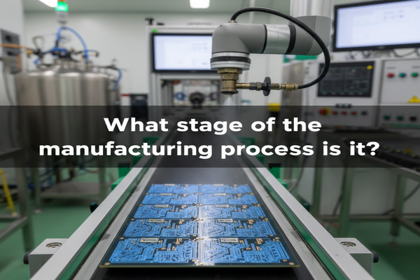
What stage of the manufacturing process is it?
Ever wonder when those tiny lines appear on a circuit board? Problems with manufacturing often come from not knowing the correct order. Learn this step and avoid costly mistakes.
PCB etching happens after the circuit pattern is defined on the board. This is usually after applying a resist layer[^2]. It comes before final assembly[^3] and testing[^4].

Let me tell you about my first time seeing a PCB being made. It was fascinating. The way each step builds on the last is truly a testament to engineering. Etching is a vital part of this sequence. It turns a plain copper board into a functional electronic component.
Understanding the Sequence
The journey from a blank copper sheet to a functional PCB involves several precise steps. Each step prepares the board for the next. Etching is positioned at a crucial point. It bridges the gap between pattern definition and component placement[^5].
- Design: Engineers create the circuit layout.
- Printing/Imaging: The circuit pattern is transferred to the copper board using a resist.
- Etching: Unwanted copper is removed.
- Stripping: The resist layer is removed.
- Drilling: Holes are made for components.
- Plating: Copper is added to holes and surfaces.
- Solder Mask: A protective layer is applied.
- Silkscreen: Labels and markings are added.
- Testing: The board is checked for functionality.
| Stage Name | Purpose | Key Action |
|---|---|---|
| Design | Create circuit blueprint | Software layout |
| Imaging | Transfer pattern onto copper | Photoresist/Print |
| Etching | Remove excess copper | Chemical bath |
| Stripping | Remove resist | Chemical removal |
| Drilling | Create holes for components | Mechanical drill |
| Plating | Enhance conductivity, prepare for solder | Electroplating |
| Solder Mask | Protect copper, define solder areas | UV exposure |
| Silkscreen | Add component labels | Ink printing |
| Testing | Verify electrical connections and function | Automated tests |
This sequence is crucial. Each part needs to be done right. If not, the final product will fail. Etching directly impacts the conductivity and integrity of the circuits. It dictates how well your device will work. Without proper etching, even the best design means nothing.
How does our PCB etching machine work?
Are you curious about the technology behind precise circuit boards? Ever faced issues with inconsistent etching results? Our machines solve these problems with advanced technology.
Our ABL PCB etching machines use a controlled chemical process[^6]. They remove copper with high precision. This ensures clean, accurate circuit traces every time.
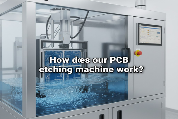
I remember the first time I saw an ABL machine in action. The level of control it offered was impressive. It changed my whole perspective on what was possible in PCB manufacturing. I'm excited to share how our specific machines achieve such excellent results.
The ABL Advantage
Our etching machines are designed for efficiency and accuracy. They use a carefully calibrated system. This system ensures uniform etching across the entire board. This means fewer errors and higher quality products for you.
- Automated Chemical Delivery: Precise control over etchant concentration.
- Uniform Spraying Systems: Ensures even exposure of the board to the etchant.
- Temperature Regulation: Maintains optimal etching conditions for consistent results.
- Integrated Rinsing: Removes etchant residues, preventing contamination.
- Waste Management: Safely collects and neutralizes spent etchants.
| Feature | Benefit | Impact on Quality |
|---|---|---|
| Precise Chemical Control | Prevents over-etching or under-etching | Accurate trace dimensions |
| Even Etchant Distribution | Uniform copper removal[^7] | Consistent board performance |
| Temperature Stability | Optimal reaction rates maintained | Predictable etching times |
| Advanced Rinsing | Eliminates chemical residue | Prevents corrosion and short circuits |
| Environmentally Friendly | Safe disposal of chemicals | Responsible manufacturing practices |
My personal experience with other machines showed me the difference. In the past, I struggled with uneven etching. This led to many scrapped boards. ABL machines, however, brought a new level of reliability. This allowed me to produce high-quality PCBs consistently. Our machines help achieve the tight tolerances needed for modern electronics. They provide a reliable and repeatable process that is crucial for mass production.
How can you get started with ABL?
Are you ready to upgrade your PCB manufacturing process? Struggling with outdated equipment? ABL offers simple solutions to boost your production quality.
Getting started with ABL is straightforward. We provide comprehensive support. This includes consultation, installation, and training. We make sure you integrate our technology smoothly.
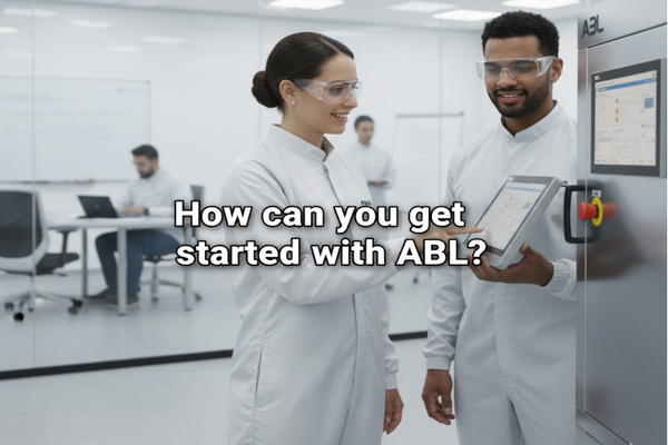
I remember when I first considered implementing new machinery. The thought was daunting. But ABL made the process surprisingly easy. Their team helped me every step of the way. I want to tell you how you can experience the same smooth transition.
Your Path to ABL Success
Transitioning to new equipment can seem complex. ABL simplifies this process for you. We have a clear, step-by-step approach. This ensures you get the most out of our etching technology. We aim to make your integration seamless.
- Initial Consultation: We discuss your needs and current setup.
- Custom Solution Design: We recommend the best machine for your specific requirements.
- Installation and Setup: Our experts install the machine at your facility.
- Operator Training: We train your team to operate and maintain the equipment.
- Ongoing Technical Support: We provide continuous help and maintenance.
| Step | Description | Your Benefit |
|---|---|---|
| Consultation | Understand your unique production goals | Tailored solution, optimal investment |
| Solution Design | Select machine models and configurations | Perfect fit for your capacity and precision |
| Installation | Professional setup and integration into your line | Minimal downtime, quick operational readiness |
| Training | Hands-on instruction for your staff | Skilled operators, maximized machine use |
| Technical Support | Immediate assistance for any operational issues | Uninterrupted production, problem resolution |
My own journey with ABL began with a simple call. I explained my production bottlenecks. Their team listened carefully. They proposed a solution that fit my budget and improved my output. The training was thorough, and their support has been consistently excellent. We found that our production efficiency increased significantly. The quality of our PCBs improved dramatically. You can achieve similar results. Just reach out to us. We will guide you through each step.
Conclusion
PCB etching precisely removes copper, forming circuits. ABL machines offer accurate, efficient etching solutions. Getting started with ABL is easy with our full support.
[^1]: Explore this resource to understand the fundamentals of PCB etching and its importance in electronics. [^2]: Understanding the role of the resist layer can enhance your knowledge of PCB production. [^3]: Gain insights into the final assembly process and its impact on PCB functionality. [^4]: Learn about the testing processes that ensure the functionality and reliability of PCBs. [^5]: Explore the techniques used for component placement to ensure optimal performance of electronic devices. [^6]: Learn about the chemical processes involved in PCB etching for better understanding of the technology. [^7]: Learn about the various methods of copper removal in PCB etching for effective circuit design.

