
Are you tired of PCB failures and short circuits? These problems often stem from one overlooked component. Learn about the unsung hero of circuit boards.
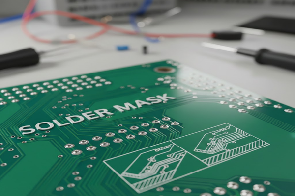
Solder mask[^1] is a protective layer on a PCB. It covers copper traces, stopping solder from going where it shouldn't. This layer prevents short circuits[^2] and protects the board from damage, making your electronics work right.
I remember the first time I saw a circuit board without a solder mask. It was a mess. Solder bridges everywhere. It made me truly appreciate what this green (or sometimes other colors) layer does. It's more than just a pretty color; it's a critical shield for your electronics.
How does solder mask affect PCB design?
Do you wonder how solder mask impacts your circuit board layout? Ignoring its role can lead to big headaches. Understand its design implications now.
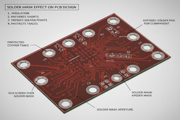
Solder mask profoundly affects PCB design[^3]. It defines where solder will and won't go, preventing short circuits. This layer ensures proper component attachment and protects the board's integrity, guiding your layout choices.

When I design PCBs, I always consider the solder mask early on. It's not an afterthought. Think about the pads for your components. The solder mask needs to open up precisely around these pads. If the opening is too small, solder might not properly wet the pad. If it’s too large, you risk exposing too much copper, which can lead to solder bridging. This becomes even more critical with fine-pitch components[^4] like BGAs or QFNs. Here, the precision of the solder mask opening, often called the solder mask defined pad[^5] or non-solder mask defined pad[^6], makes a huge difference. A non-solder mask defined pad means the copper pad is larger than the solder mask opening, giving more surface area for solder. A solder mask defined pad means the solder mask slightly overlaps the copper pad, constraining the solder to a specific area. Each approach has its benefits and drawbacks for different component types and manufacturing processes. We also need to think about clearances. The space between solder mask features and exposed copper is vital. Insufficient clearance can cause manufacturing defects.
| Feature Type | Description | Design Consideration |
|---|---|---|
| Solder Mask Opening | Area where solder paste is applied | Must align perfectly with component pads |
| Solder Mask Dam | Material between adjacent pads | Prevents solder bridging, especially on fine pitch |
| Solder Mask Clearance | Space between mask and copper trace | Ensures isolation and prevents exposure issues |
| Solder Mask Defined Pad | Mask slightly overlaps copper pad | Good for constraining solder on small pads |
| Non-Solder Mask Defined Pad | Mask opening smaller than copper pad | Provides more surface for solder attachment |
How thick should solder mask be on PCB?
Are you unsure about the ideal solder mask thickness for your PCB? The wrong thickness can lead to manufacturing issues. Find out the right specifications.
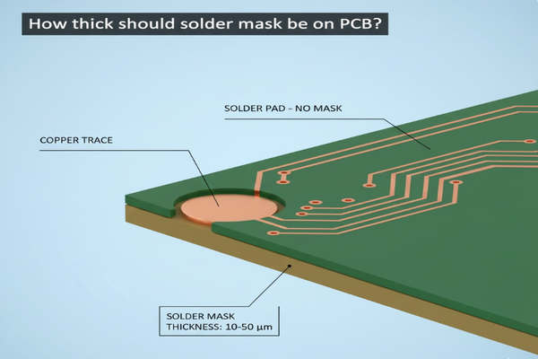
Solder mask thickness varies but typically ranges from 10 to 50 micrometers. This thickness offers sufficient insulation and protection. The exact requirement depends on factors like copper thickness and component density, ensuring optimal performance and durability.

I've learned that solder mask thickness is a delicate balance. Too thin, and it might not offer enough protection against environmental factors or electrical breakdown. It also won't effectively prevent solder bridging. Too thick, and you could run into problems during assembly, especially with small features or vias. For example, if the solder mask is too thick over a small via, it might not fully cure or could lead to inconsistent openings. The typical range I work with is around 25 to 35 micrometers over the copper traces. Over the bare laminate, it might be thicker, closer to 50 micrometers. This difference occurs because the mask flows into the valleys between the traces. The thickness also depends on the application method. Liquid Photoimageable Solder Mask[^7] (LPSM), which is very common, offers good control over thickness and resolution. Dry film solder mask can be thicker and is often used for specific applications requiring greater mechanical protection. Always check with your PCB manufacturer for their recommended thickness, as their process capabilities will influence the best choice. Different colors of solder mask can also affect perceived thickness, though the actual functional thickness is what matters.
| Solder Mask Type | Typical Thickness (micrometers) | Application Method | Key Characteristics |
|---|---|---|---|
| Liquid Photoimageable (LPSM) | 10-50 | Screen printing, curtain coating, spray coating | High resolution, most common, good for fine features |
| Dry Film (DFSM) | 50-100+ | Lamination | High mechanical protection, often thicker |
| Thermal Cure Solder Mask | 25-75 | Screen printing | Good chemical resistance, traditional |
| UV Cure Solder Mask | 15-40 | Screen printing | Fast curing, cost-effective for some uses |
What can I use instead of a solder mask?
Are you exploring alternatives to traditional solder mask? Sometimes, the standard solution isn't suitable. Discover other options available.
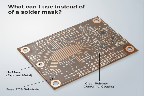
While solder mask is standard, alternatives exist for specific needs. Conformal coatings offer environmental protection. Other options like temporary peelable masks can protect specific areas during processing. These alternatives serve niche applications where a permanent solder mask isn't ideal.

I've encountered situations where a traditional solder mask wasn't the best fit. For example, in high-frequency applications, the dielectric properties of standard solder mask can sometimes impact signal integrity. In such cases, designers might choose to use a thinner mask or even no mask in critical areas, relying on other protective measures. Conformal coatings are a big alternative. These are typically applied after assembly to protect the entire board from moisture, dust, chemicals, and extreme temperatures. They come in various chemistries, like acrylic, silicone, urethane, and parylene. Each has its own benefits regarding flexibility, chemical resistance, and ease of rework. Another option I've used is a temporary peelable solder mask. This isn't a permanent replacement but is incredibly useful during manufacturing. It protects specific areas, like connectors or keep-out zones, from solder or conformal coating during processing. After the process, you simply peel it off. For very high-density interconnect (HDI) boards or flex circuits, sometimes specialized polyimide layers are used, which can offer both protection and structural integrity. Each alternative has its trade-offs in terms of cost, application process, and protective qualities.
| Alternative | Primary Function | Application Stage | Pros | Cons |
|---|---|---|---|---|
| Conformal Coating | Environmental protection | Post-assembly | Flexible, chemical resistance | Can be difficult to rework, adds thickness |
| Temporary Peelable Mask | Process protection | During assembly | Easy to remove, targeted protection | Not permanent, only for manufacturing |
| No Solder Mask | Specific electrical needs | Design decision | Lower dielectric constant | No solder bridging protection, exposed copper |
| Polyimide Layer | Protection and structure | Fabrication/Assembly | High temperature, flexible | More complex process, higher cost |
| Encapsulants | Mechanical protection | Post-assembly | Robust protection | Permanent, difficult rework |
Conclusion
Solder mask is vital for PCBs, preventing shorts and offering protection. Its thickness and alternatives vary by design needs. Understanding it ensures reliable circuit boards.
[^1]: Explore the importance of solder mask in PCB design and how it prevents failures. [^2]: Understand the common causes of short circuits in PCBs and how to prevent them. [^3]: Learn how effective PCB design can enhance electronic performance and reliability. [^4]: Explore the challenges and considerations of using fine-pitch components. [^5]: Learn about solder mask defined pads and their significance in PCB layouts. [^6]: Explore the concept of non-solder mask defined pads and their benefits. [^7]: Find out about Liquid Photoimageable Solder Mask and its applications.

