
Confused by PCB terms? Many people are. Understanding the right board for your electronics project can save time and money.
A Zero PCB[^1] (perforated board) has pre-drilled holes and copper pads for manual wiring. A blank PCB[^2] is a plain copper-clad board[^3] that needs etching[^4] to form circuits. I learned this difference early in my DIY electronics journey.
When I first started building circuits, I quickly realized there were different types of circuit boards, and choosing the wrong one could lead to headaches. It's crucial to know the distinction to pick the right foundation for your project. Let's dig into what sets these two apart.
What is the structure of a bare PCB?
Ever wondered what a bare PCB is made of? It's more than just a green board. Knowing its layers helps you understand how circuits work.
A bare PCB, or blank PCB, typically consists of an insulating substrate (like fiberglass) covered with a copper layer on one or both sides. This copper is later etched away to create the circuit traces. I remember examining my first bare board, wondering how it would become a complex circuit.
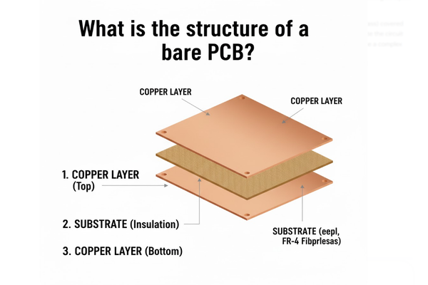
Let's break down the layers of a bare PCB. Understanding each part helps clarify its function.
Substrate Material
The core of the PCB is the substrate. This is often made from fiberglass (FR-4).
- Insulation: It provides electrical insulation between layers.
- Mechanical Support: It gives the board its rigidity and shape.
- Heat Resistance: FR-4 can withstand high temperatures during soldering.
Copper Layer
This is the conductive part where circuits are formed.
- Conductivity: Copper is an excellent conductor of electricity.
- Thickness: The copper thickness varies, usually measured in ounces per square foot. Thicker copper handles more current.
Manufacturing Process
The journey from blank to functional PCB involves several steps.
- Lamination: Copper foil is laminated onto the substrate under heat and pressure.
- Etching: A photographic process removes unwanted copper, leaving only the circuit traces.
| Component | Material | Function |
|---|---|---|
| Substrate | FR-4 | Insulation, mechanical support |
| Copper Layer | Copper | Electrical conduction, circuit traces |
| Prepreg | Epoxy resin | Binds layers in multi-layer PCBs[^5] |
| Solder Mask | Polymer | Protects copper, prevents solder bridges |
What are the different types of blank PCBs?
Did you know blank PCBs aren't all the same? Different types serve different purposes. Choosing wisely impacts your project's success.
Blank PCBs come in single-sided, double-sided, and multi-layer variations, primarily defined by the number of copper layers. Zero PCBs, or perforated boards, are also a type of blank board for prototyping, featuring pre-drilled holes and individual copper pads. I've used all these types for different projects.
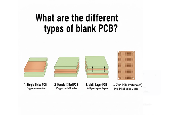
Understanding the different types of blank PCBs helps you choose the correct one for your specific application. Each type has its own advantages and uses.
Single-Sided PCBs
These are the simplest and most common.
- Description: One layer of copper on one side of the substrate.
- Use Cases: Simple electronics, low-cost products, learning projects.
- Advantages: Easy to design and manufacture, cost-effective.
Double-Sided PCBs
These offer more flexibility for complex circuits.
- Description: Copper layers on both sides of the substrate. Holes (vias) connect traces between layers.
- Use Cases: More complex circuits, medium-density component placement.
- Advantages: Higher component density, more compact designs.
Multi-Layer PCBs
For highly complex and miniature electronics.
- Description: More than two copper layers, separated by insulating layers, all laminated together.
- Use Cases: Computers, smartphones, high-frequency circuits.
- Advantages: Very high component density, reduced noise, smaller size.
Zero PCBs (Perforated Boards)
These are for quick, manual prototyping.
- Description: A non-conductive board with a grid of pre-drilled holes, each with a small copper pad.
- Use Cases: Rapid prototyping, hobby projects, manual circuit assembly.
- Advantages: No etching required, easy to modify circuits.
| PCB Type | Copper Layers | Complexity | Typical Use Cases |
|---|---|---|---|
| Single-Sided | 1 | Low | Simple gadgets, LED circuits |
| Double-Sided | 2 | Medium | Microcontroller boards, power supplies |
| Multi-Layer | 4+ | High | Computers, mobile devices |
| Zero PCB | N/A | Manual wiring | Prototyping, hobby projects |
How can I make a blank PCB at South-Electronic?
Thinking of getting a custom blank PCB made? You might wonder how it's done. At South-Electronic, the process is streamlined and precise.
To make a blank PCB at South-Electronic, you'd typically submit your design files (Gerber files[^6]). They then use advanced manufacturing processes like photolithography and chemical etching to create your custom board based on your specifications. I've seen how precise their work is.
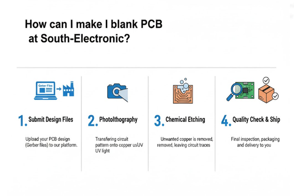
Dive deeper Paragraph: Let's walk through the general steps involved in making a blank PCB, focusing on how a professional manufacturer like South-Electronic would approach it.
Design Submission
The first step is always your design.
- Gerber Files: You provide your circuit design in Gerber format, which is the industry standard for PCB manufacturing. This includes all layers, drill files, and outlines.
- Specifications: You also specify material type, copper thickness, solder mask[^7] color, and surface finish.
Manufacturing Process
South-Electronic uses state-of-the-art equipment.
- Material Preparation: The process starts with cutting the substrate material[^8] to size.
- Imaging: A photosensitive resist is applied to the copper surface. Your circuit pattern is then exposed onto this resist using UV light.
- Etching: Chemical solutions etch away the unwanted copper, leaving only your circuit traces.
- Drilling: Holes for components and vias are precisely drilled using automated machines.
- Plating: For double-sided and multi-layer PCBs, holes are plated with copper to create electrical connections between layers.
Quality Control
Every step includes rigorous checks.
- Automated Optical Inspection (AOI): Machines scan the boards for defects, shorts, and open circuits.
- Electrical Testing: Boards are tested to ensure all connections are correct and there are no shorts or open circuits.
- Final Inspection: A thorough visual check ensures the finished product meets all specifications.
| Step | Description | Output |
|---|---|---|
| Design Submission | Provide Gerber files and specifications | Ready-to-manufacture digital blueprint |
| Imaging & Etching | Transfer design onto copper, remove excess | Copper traces formed |
| Drilling & Plating | Create holes and interconnect layers | Electrically connected layers |
| Quality Control | Inspect and test for defects and functionality | High-quality, functional PCB |
Conclusion
Zero PCBs are for manual prototyping, while blank PCBs are etched to create circuits. Knowing the difference helps in choosing the right board for your electronics project.
[^1]: Explore the unique features of Zero PCBs and how they can simplify your prototyping process. [^2]: Learn about blank PCBs and their role in creating custom electronic circuits. [^3]: Understand the significance of copper-clad boards in the PCB manufacturing process. [^4]: Dive into the etching process and its importance in creating circuit traces. [^5]: Explore the advantages of multi-layer PCBs for high-density electronic applications. [^6]: Learn about Gerber files and their importance in the PCB manufacturing process. [^7]: Understand the role of solder masks in protecting PCB traces and ensuring reliability. [^8]: Explore different substrate materials and their impact on PCB performance.

