
What is the difference between EDA with PCB?
EDA (Electronic Design Automation) involves software tools for designing, simulating, and verifying electronic circuits, streamlining the creation process from concept to implementation. In contrast, a PCB (Printed Circuit Board) is a physical board that supports and electrically connects electronic components, serving as the foundation for constructing electronic devices. While EDA tools focus on the design and validation phase, PCBs are crucial during the manufacturing phase, providing the physical structure and connections necessary for the electronic circuits to function.
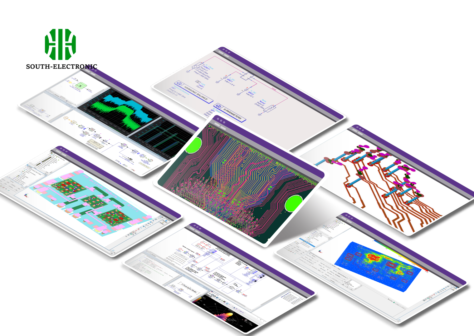
What is EDA software?
EDA is electronic design automation, which is the abbreviation of Electronic Design Automation in English. It refers to the design method of using computer-aided design (CAD) software to complete the functional design, synthesis, verification, physical design (including layout, wiring, layout, design rule checking, etc.) of very large-scale integrated circuit (VLSI) chips.
What are the common EDA tools?
1.Protel
PROTEL is an EDA software launched by Altium in the late 1980s. Among the CAD software in the electronics industry, it deservedly ranks ahead of many EDA software and is the preferred software for electronic designers. It has been used in China for a long time and has the highest popularity in China. Some colleges and universities have specially opened courses to learn it. Almost all electronic companies need to use it. Many large companies often write the requirement to use PROTEL in their conditions when recruiting electronic design talents.
2.Altium Designer
Altium Designer is an integrated electronic product development system launched by Altium, the original developer of Protel software, and mainly runs on the Windows operating system. This software provides designers with a new design solution by perfectly integrating technologies such as schematic design, circuit simulation, PCB drawing and editing, topology logic automatic routing, signal integrity analysis and design output, allowing designers to easily design. Proficient use of this software will greatly improve the quality and efficiency of circuit design.
3.Cadence
Cadence Design Systems, Inc; NASDAQ: CDNS is a software company specializing in electronic design automation (EDA).
The Cadence Allegro system interconnect platform can collaboratively design high-performance interconnects across integrated circuits, packages and PCBs.
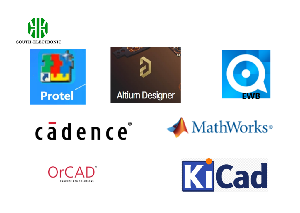
4.Kicad
KiCad is a GPL EDA (Electronic Design Automation) software package that can be used as an alternative version of protel under Linux.
5.OrCAD
OrCAD is an electronic design automation software package for personal computers, specifically designed for electronic engineers to design circuit diagrams and related diagrams, design printed circuit boards for printed circuit board printing, and simulate circuits.
6.MATLAB
MATLAB is a commercial mathematical software produced by MathWorks in the United States. It is an advanced technical computing language and interactive environment for algorithm development, data visualization, data analysis and numerical calculation. It mainly includes two parts: MATLAB and Simulink.
It integrates many powerful functions such as numerical analysis, matrix calculation, scientific data visualization, and modeling and simulation of nonlinear dynamic systems in an easy-to-use window environment, providing a comprehensive solution for scientific research, engineering design and many scientific fields that must perform effective numerical calculations. It has largely gotten rid of the editing mode of traditional non-interactive programming languages (such as C and Fortran) and represents the advanced level of international scientific computing software today.
7.EWB
EWB software, the full name of ELECTRONICS WORKBENCH EDA, is an EDA software launched by Interactive Image Technology Co., Ltd. in the early 1990s. It is used for mixed simulation of analog circuits and digital circuits. It can be used to see the output waveforms of various circuits directly on the screen. EWB is a small but powerful simulation software.
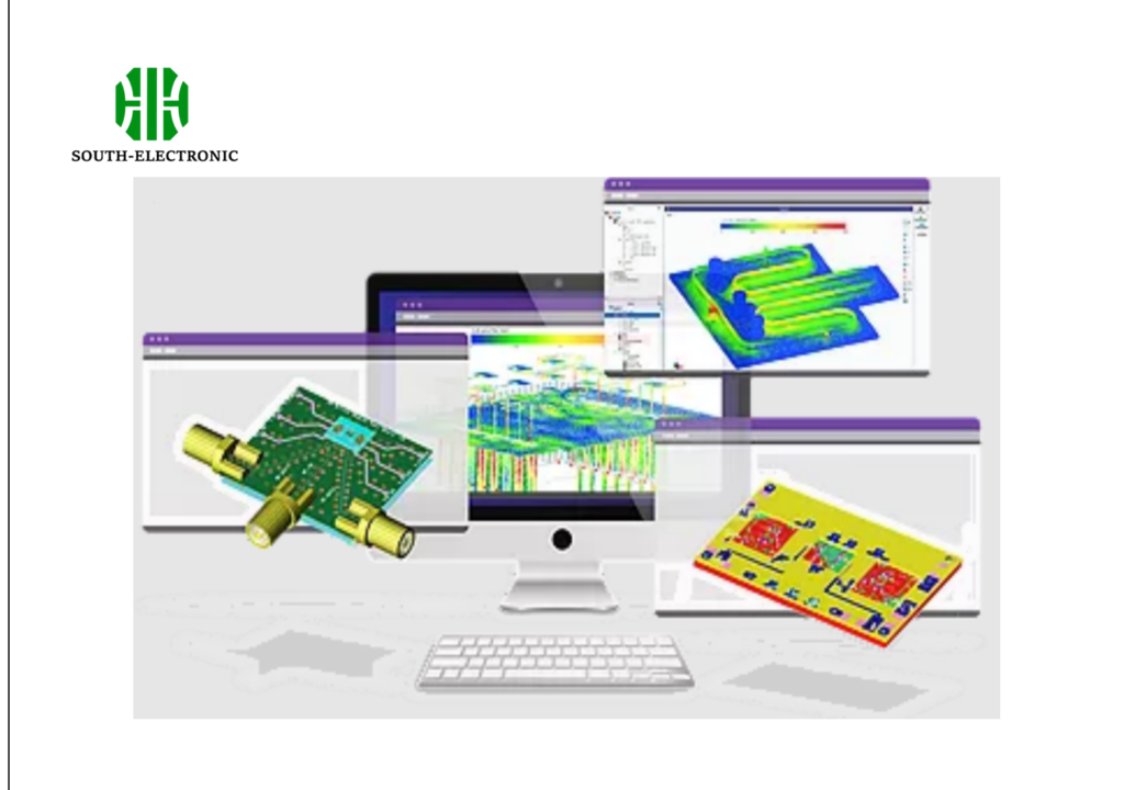
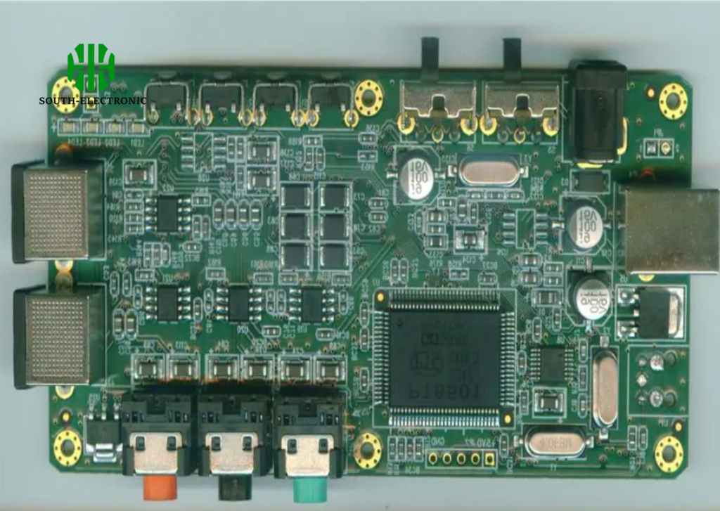
What is PCB?
PCB (Printed Circuit Board) refers to a printed board with point-to-point connections and printed components on a general substrate according to a predetermined design. It is the support for electronic components and the carrier for the electrical connection of electronic components.
To understand the concept of printed circuit boards, we first need to distinguish between PCB and PCBA.
The circuit boards we usually see are all components welded on the basis of PCB, that is, PCBA (PCB Assembly). PCB is a “bare board” or “bare board”, that is, PCB is a circuit board before components are welded. PCB and circuit components are processed and assembled to form a circuit board actually used in electronic products.
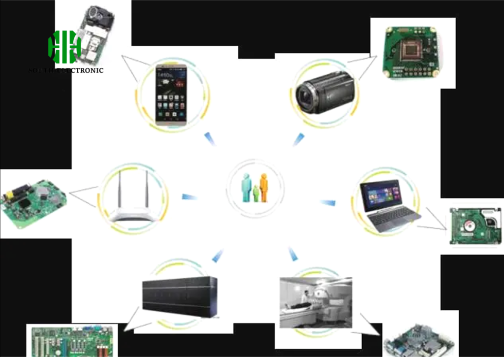
PCB is closely related to people’s daily life, from the small mobile phones, digital cameras, and laptops that individuals often use, to the wireless routers and desktop computers that families often use, to the large medical equipment such as MRI used in hospitals, wireless base stations used by telecom operators, data center servers and other products, all of which require PCB.
The origin and history of PCB
- In 1925, Charles Ducas of the United States printed circuit patterns on an insulating substrate, and then used electroplating to build conductors. This is a sign of the opening of the current PCB technology.
- In 1947, epoxy resin began to be used to manufacture substrates.
- In 1953, Motorola developed a double-sided board with electroplated through-holes, which was later applied to multi-layer circuit boards.
- In 1960, V. Dahlgreen used metal foil films with printed circuits to stick to plastic to make flexible printed circuit boards.
- In 1961, Hazeltine Corporation of the United States referred to the electroplated through-hole method to make multi-layer boards.
- In 1995, Panasonic developed the ALIVH build-up printed circuit board.
- In 1996, Toshiba developed the B2IT build-up printed circuit board.
- At the end of the 20th century, new technologies such as Rigid-Flex, buried resistors, buried capacitors, and metal substrates emerged. PCB is not only a carrier for completing the interconnection function, but also an extremely important component in all electronic products, playing a vital role in today’s electronic products.
Best Practices Summary
While EDA tools and PCB are both essential in the creation of electronic devices, they serve different roles. EDA tools are used for the design and verification of electronic circuits, while PCBs are the physical entities that host these circuits. Understanding the distinction and interplay between EDA and PCB is crucial for anyone involved in electronic design and manufacturing.

