
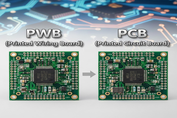
You're wondering about PWB vs. PCB, right? It's a common question that can cause confusion in electronics. Don't worry, I've got you covered.
While "PWB" and "PCB" are often used interchangeably today, "PWB" (Printed Wiring Board[^1]) was historically for basic wiring, and "PCB" (Printed Circuit Board[^2]) evolved with etched circuits. Now, PCB is the global standard, though PWB is still used in some regions like Japan.
Let's dive into the core of these terms and clear up any lingering questions you might have. You'll see how understanding this distinction can help you in the electronics world.
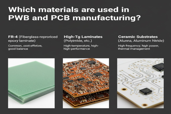
Which materials are used in PWB and PCB manufacturing?
Ever wondered what goes into making these boards? The materials are crucial for how they perform. If you pick the wrong ones, your circuit might fail.
PWB and PCB manufacturing commonly use materials like FR-4 (fiberglass-reinforced epoxy laminate), which balances cost and performance, and specialized materials such as high-Tg (high glass transition temperature) laminates or ceramic substrates for demanding applications.
Dive deeper into materials used:
Substrate Materials
The foundation of any board is its substrate. This provides mechanical support and electrical insulation.
| Material Type | Characteristics | Common Applications |
|---|---|---|
| FR-4[^3] | Standard, good balance of electrical/mechanical properties, cost-effective | General electronics, consumer devices |
| High-Tg Laminates[^4] | Higher heat resistance, better dimensional stability | High-power applications, automotive, aerospace |
| Polyimide[^5] | Flexible, high-temperature resistance | Flexible circuits, medical devices |
| Ceramic Substrates[^6] | Excellent thermal conductivity, high-frequency performance | RF/microwave circuits, power modules |
Conductive Materials
Copper is king here. It forms the traces that carry electrical signals.
- Electrolytic Copper: Most common, excellent conductivity.
- Rolled Annealed Copper: Used in flexible circuits for better flexibility.
Solder Mask
This protective layer prevents short circuits and corrosion.
- Epoxy-based: Standard, green in color, offers good protection.
- Liquid Photoimageable (LPI): Allows for finer features and better precision.
Legend Ink
Also known as silkscreen, this adds component designators and markings.
- Epoxy-based Ink: Durable, typically white or black.
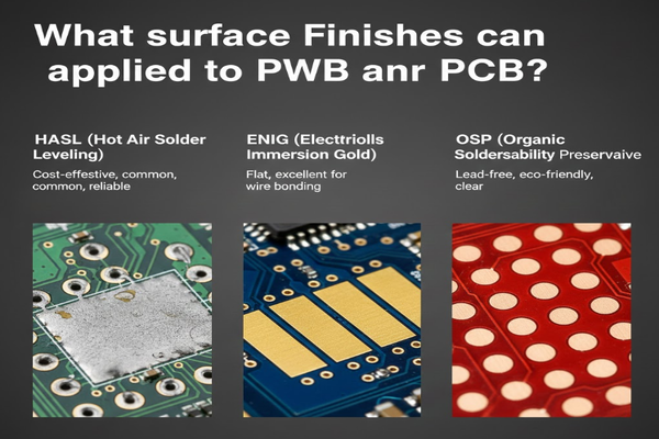
What surface finishes can be applied to PWB or PCB?
Are you curious about the final layer on your circuit board? The surface finish is more than just cosmetic; it's vital for soldering and protection.
Surface finishes on PWBs and PCBs protect exposed copper from oxidation and improve solderability. Common types include HASL[^7] (Hot Air Solder Leveling) for cost-effectiveness, ENIG[^8] (Electroless Nickel Immersion Gold) for flat surfaces and wire bonding, and OSP[^9] (Organic Solderability Preservative) for lead-free processes.
The Role of Surface Finishes
Surface finishes are critical. They protect the copper traces from oxidation, which can ruin solder joints. They also ensure a good electrical connection during assembly.
| Finish Type | Advantages | Disadvantages | Applications |
|---|---|---|---|
| HASL (Hot Air Solder Leveling) | Cost-effective, good solderability | Uneven surface, thermal shock risk | General purpose, automotive |
| ENIG (Electroless Nickel Immersion Gold) | Flat surface, good for fine pitch, excellent shelf life, good for wire bonding | Higher cost, "black pad" risk | BGA, fine pitch, medical, aerospace |
| OSP (Organic Solderability Preservative) | Environmentally friendly, very flat, simple process | Limited shelf life, sensitive to handling | Consumer electronics, lead-free applications |
| Immersion Silver (ImAg) | Flat surface, good for fine pitch, low signal loss | Tarnish risk, poor handling resistance | RF/microwave, high-speed applications |
| Immersion Tin (ImSn) | Flat surface, good solderability | Whisker growth risk, short shelf life | Press-fit connectors, lead-free applications |
Key Considerations
When choosing a finish, think about:
- Cost: Some finishes are much more expensive.
- Solderability: How well components will attach.
- Shelf Life: How long the board can be stored before assembly.
- Reliability: How it performs over time, especially in harsh environments.
- Environmental Impact: Lead-free options are becoming standard.
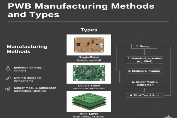
PWB Manufacturing Methods and Types
Have you ever wondered how these complex boards are actually made? The methods directly impact what the board can do.
PWB and PCB manufacturing involves processes like etching conductive patterns from copper foil laminated onto a substrate, drilling holes for components and interconnections, and applying solder mask and silkscreen. Boards can be single-sided, double-sided, or multi-layered, depending on circuit complexity.
Basic Manufacturing Steps
Making a circuit board is a multi-step dance. Each step is precise.
- Design: Engineers create the layout using specialized software.
- Material Preparation: Copper-clad laminates are cut to size.
- Imaging: The circuit pattern is transferred to the copper using photolithography.
- Etching: Unwanted copper is removed, leaving the circuit traces.
- Drilling: Holes are drilled for components and vias (interconnections between layers).
- Plating: Copper is deposited into holes and on traces to improve conductivity.
- Solder Mask Application: A protective layer is applied.
- Silkscreen: Component identifiers are printed.
- Surface Finish: The final protective layer is added.
- Testing: Electrical tests verify functionality.
- Fabrication: Individual boards are cut from the panel.
Types of Boards
Different needs call for different board types.
| Type | Description | Advantages | Disadvantages |
|---|---|---|---|
| Single-Sided | Conductive pattern on one side only | Simple, low cost | Low density, limited complexity |
| Double-Sided | Conductive patterns on both sides, connected by plated through-holes | Increased density, more complex circuits | More complex than single-sided |
| Multi-Layer | Multiple layers of circuitry separated by insulation, interconnected by vias | High density, complex circuits, reduced size | High cost, complex manufacturing |
| Flexible PCBs (Flex) | Built on flexible plastic substrates | Can bend, save space, shock resistance | Higher cost, delicate handling |
| Rigid-Flex PCBs | Combination of rigid and flexible sections | Best of both worlds, ideal for compact devices | Very high cost, complex design |
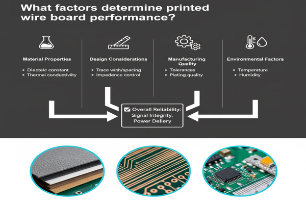
What factors determine printed wire board performance?
Are you wondering what makes a circuit board truly effective? Its performance depends on a mix of critical factors. Overlooking any of these can lead to major issues.
Printed wire board performance is determined by material properties (dielectric constant, thermal conductivity), design considerations (trace width, impedance control), manufacturing quality (tolerances, plating), and environmental factors (temperature, humidity). These elements collectively influence signal integrity, power delivery, and overall reliability.
Electrical Characteristics
These are paramount for signal integrity.
- Dielectric Constant (Dk): Affects signal speed and impedance. Lower Dk often means faster signals.
- Loss Tangent (Df): Represents signal loss. Lower Df is better for high-frequency applications.
- Impedance Control: Maintaining consistent impedance along signal paths prevents reflections and signal degradation. This is crucial for high-speed data.
- Trace Width and Spacing: Determines current carrying capacity and prevents crosstalk between adjacent traces.
Thermal Management
Heat is the enemy of electronics.
- Thermal Conductivity: How well the material conducts heat away from components.
- Thermal Expansion (CTE): How much the material expands with heat. Mismatched CTEs between materials can cause stress and failures.
- Thermal Resistance: Measures a material's ability to resist heat flow.
Mechanical Integrity
The board needs to hold up physically.
- Flexural Strength: Resistance to bending.
- Peel Strength: How well copper adheres to the substrate.
- Dimensional Stability: How much the board changes size with temperature or humidity.
Environmental Robustness
How the board handles the real world.
- Moisture Absorption: High moisture can affect electrical properties and reliability.
- Chemical Resistance: Protection against harsh environments.
- Flammability (UL 94 rating): How easily the material ignites and spreads flame.
Conclusion
While "PWB" and "PCB" might sound similar, this article clarifies their distinctions, materials, manufacturing, finishes, and performance factors.
[^1]: Explore this link to understand the historical context and applications of Printed Wiring Boards in electronics. [^2]: Learn about the evolution and significance of Printed Circuit Boards in modern electronics. [^3]: Discover why FR-4 is the go-to material for most circuit boards and its advantages. [^4]: Find out how High-Tg Laminates enhance performance in high-temperature applications. [^5]: Learn about the benefits of Polyimide in flexible circuits and high-temperature environments. [^6]: Explore the unique properties of Ceramic Substrates and their applications in high-frequency circuits. [^7]: Learn about the cost-effectiveness and applications of HASL in circuit board manufacturing. [^8]: Explore the advantages of ENIG for fine pitch applications and its long shelf life. [^9]: Find out how OSP provides environmentally friendly options for lead-free applications.

