
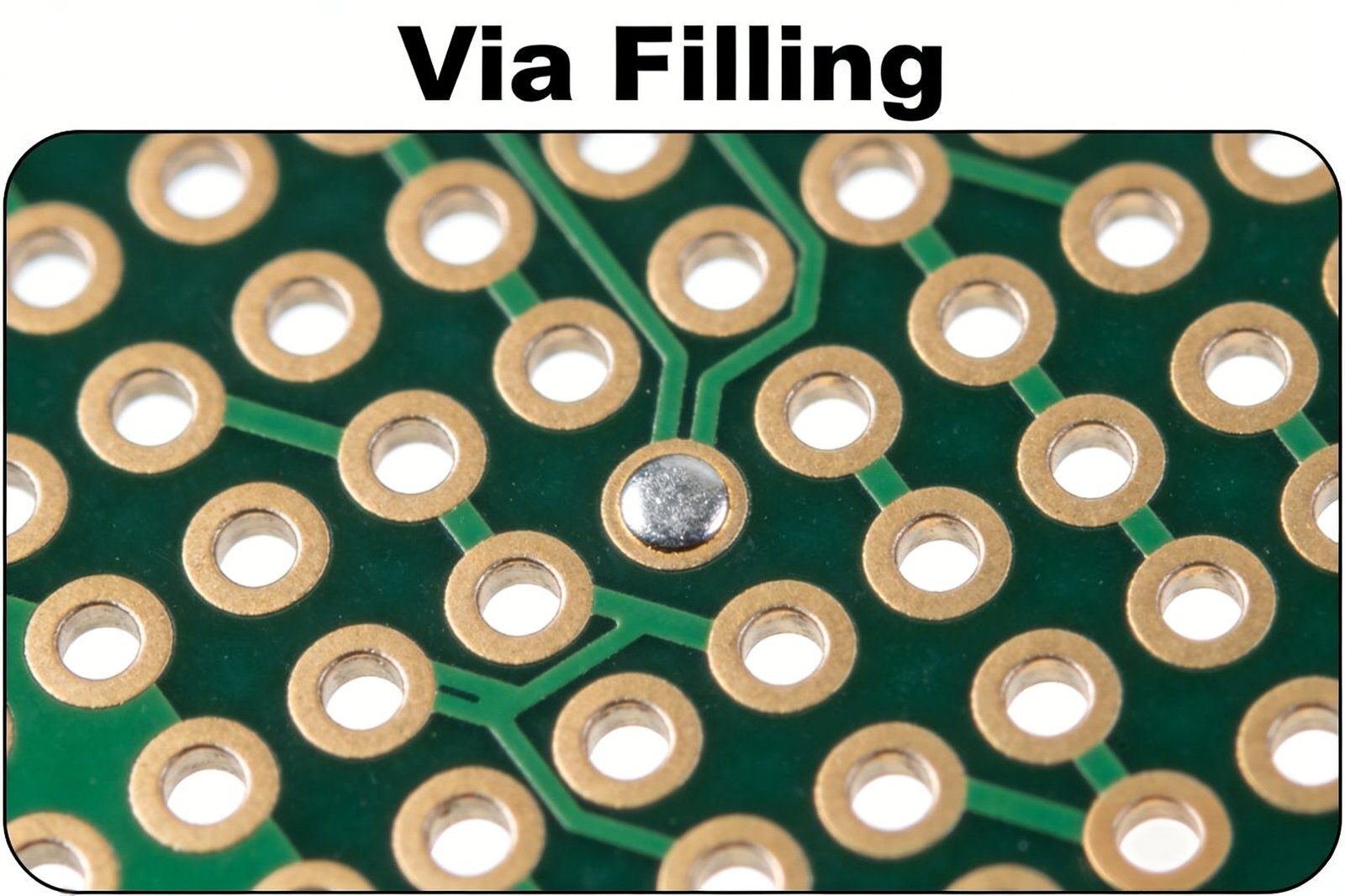
Via filling may be essential for your PCB reliability, but what does it really involve?
Via filling in PCB manufacturing completely fills plated through-holes with materials, improving reliability and preventing issues like air or moisture entrapment.
To truly understand via filling, we first need to consider its processes and benefits. This will help you appreciate why this technique is critical in PCB manufacturing. Let's explore it in detail.
How is via filling done with resin?
Ever wondered how resin effortlessly fills those small holes in your circuit boards?
Via filling with resin involves preparing the PCB, applying the resin, and curing it to ensure a solid fill. This process enhances the board's reliability without compromising its integrity.
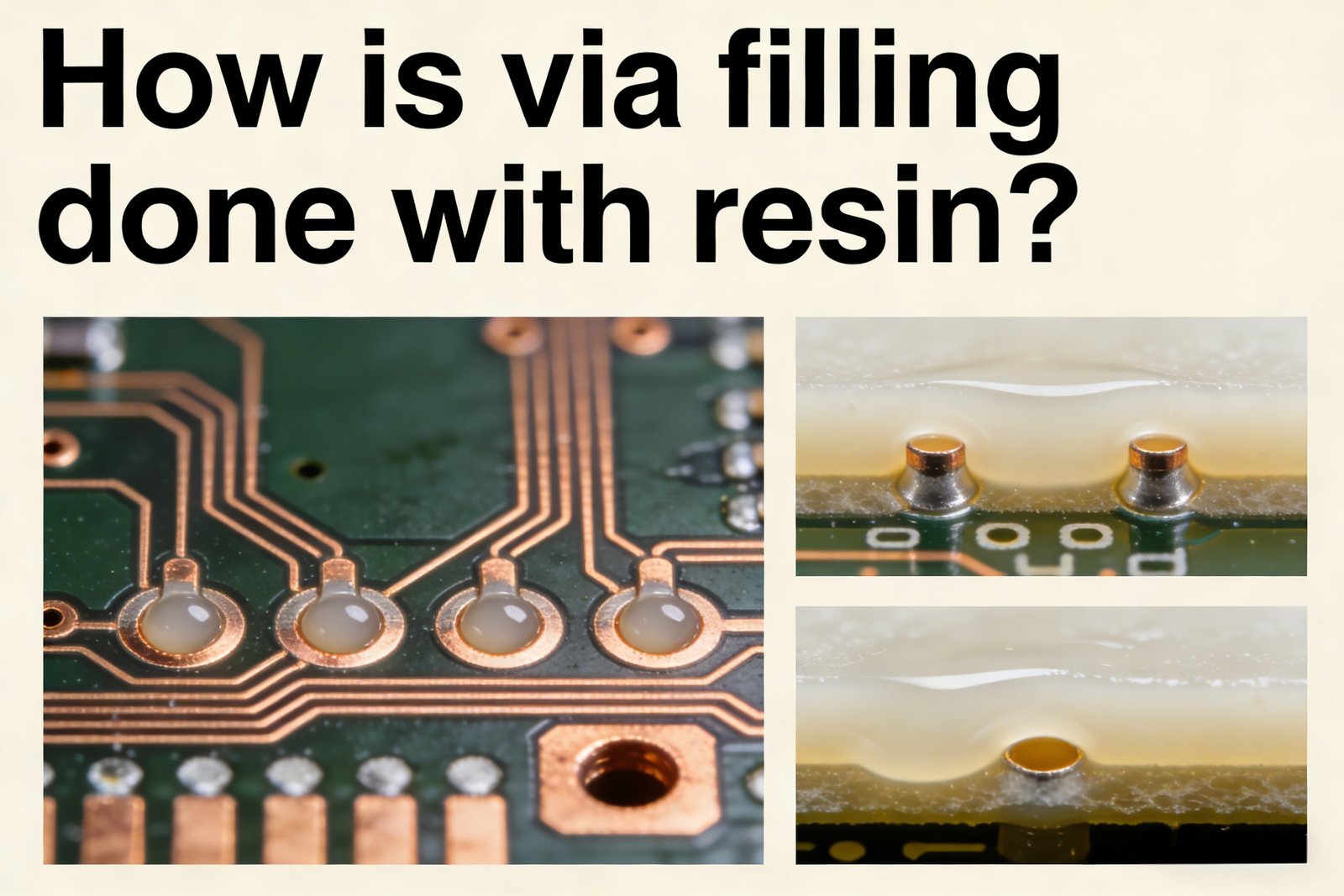
In PCB manufacturing, via filling with resin is a key method of enhancing performance. The process generally follows these steps:
- Preparation: Ensure the PCB is clean and free of contaminants.
- Filling: Apply resin into the vias using techniques like syringe dispensing.
- Curing: Use heat or UV light to harden the resin, ensuring a solid fill.
Using resin is beneficial because it prevents moisture intrusion and enhances mechanical strength.
| Step | Description |
|---|---|
| Preparation | Cleaning the PCB for optimal adhesion |
| Filling | Injecting resin until vias are fully filled |
| Curing | Hardening the resin with a heat or UV cure |
What are the technical specifications for via filling?
Do technical details about via filling confuse you?
Understanding the specifications for via filling helps ensure optimal performance and reliability. Key parameters include material type, fill depth, and curing conditions.
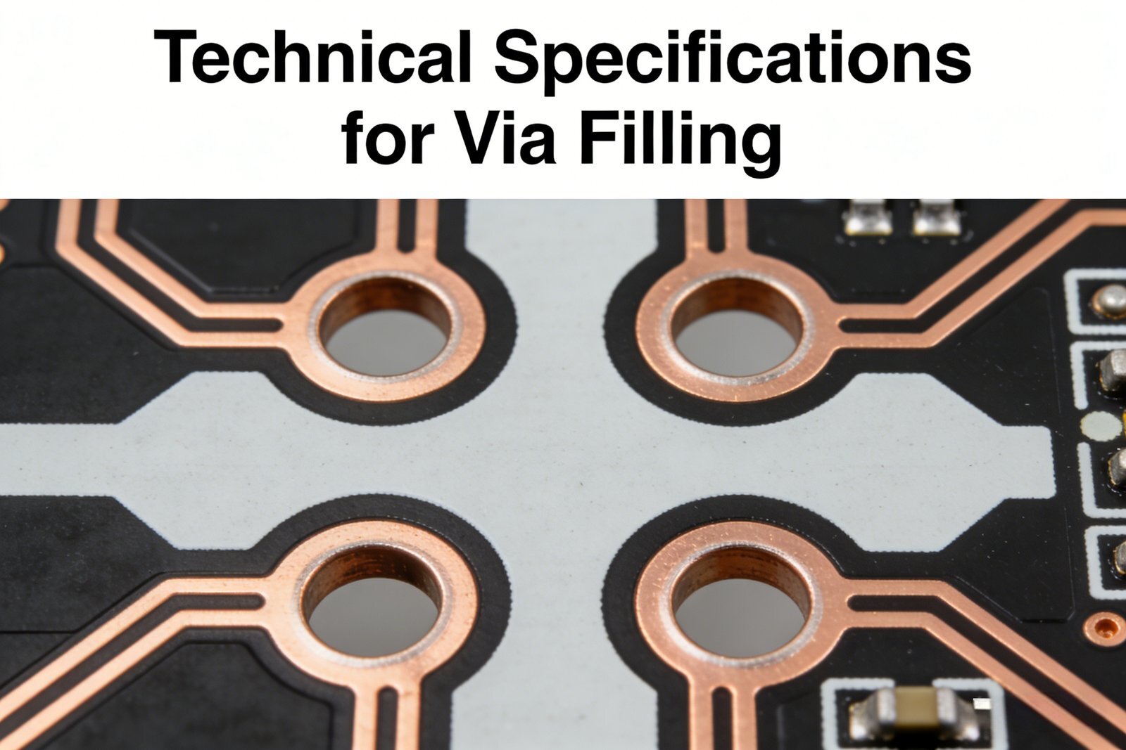
Via filling has specific technical specifications that must be adhered to for effective results. These include:
- Material Characteristics: Choose conductive or non-conductive materials based on application needs.
- Fill Depth and Diameter: Ensure the fill depth matches your PCB requirements.
- Curing Temperature: Follow recommended temperature ranges for resin curing to avoid defects.
Here's a detailed comparison based on these specifications:
| Specification | Details |
|---|---|
| Material Used | Copper, silver-filled epoxy, or insulating resin |
| Fill Depth | Should generally match the diameter of the via |
| Curing Conditions | Typically between 100-150°C for effective results |
How can we avoid naming confusion between via filling and via plugging?
Is the difference between via filling and plugging clear enough for you?
Avoiding naming confusion between via filling and via plugging is essential for clear communication. Both processes involve filling vias, but their purposes and methods differ.
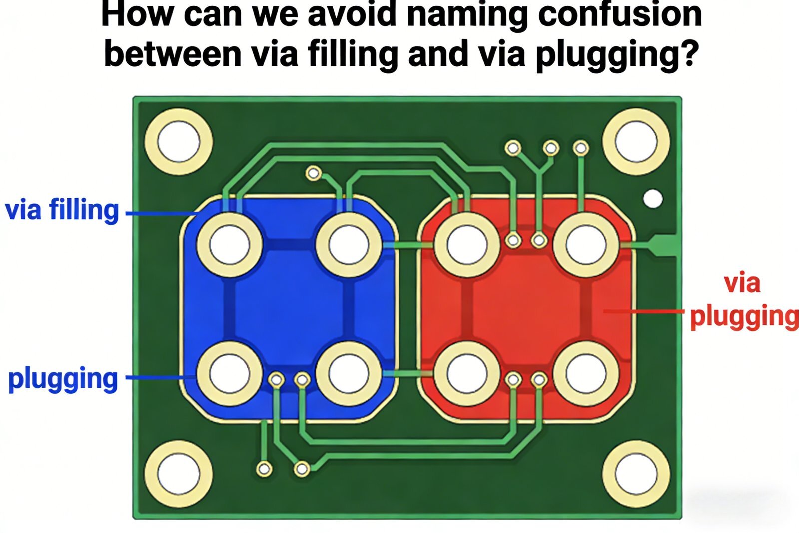
To clarify the distinction, consider the following:
-
Purpose:
- Via Filling: Completes holes for connectivity or thermal performance.
- Via Plugging: Blocks vias to prevent solder flow during assembly.
-
Materials:
- Via Filling: Uses conductive (copper) or non-conductive materials (epoxy).
- Via Plugging: Generally non-conductive materials to prevent solder ingress.
-
Process:
- Via Filling: Focuses on enhancing conductivity and thermal management.
- Via Plugging: Primarily concerned with mechanical stability during assembly.
Here's a comparison table for clarity:
| Parameter | Via Filling | Via Plugging |
|---|---|---|
| Purpose | Enhances circuit performance | Prevents solder flow |
| Materials | Conductive/non-conductive fillers | Non-conductive materials |
| Applications | High-density interconnections | Basic assembly stability |
In summary, knowing the specifications and differences between the two terms can eliminate confusion and improve communication among PCB manufacturers and clients.
Conclusion, via filling is a crucial process in PCB manufacturing that enhances reliability, prevents moisture entrapment, and improves mechanical strength. Understanding its importance and distinctions can significantly impact your PCB's performance.


