
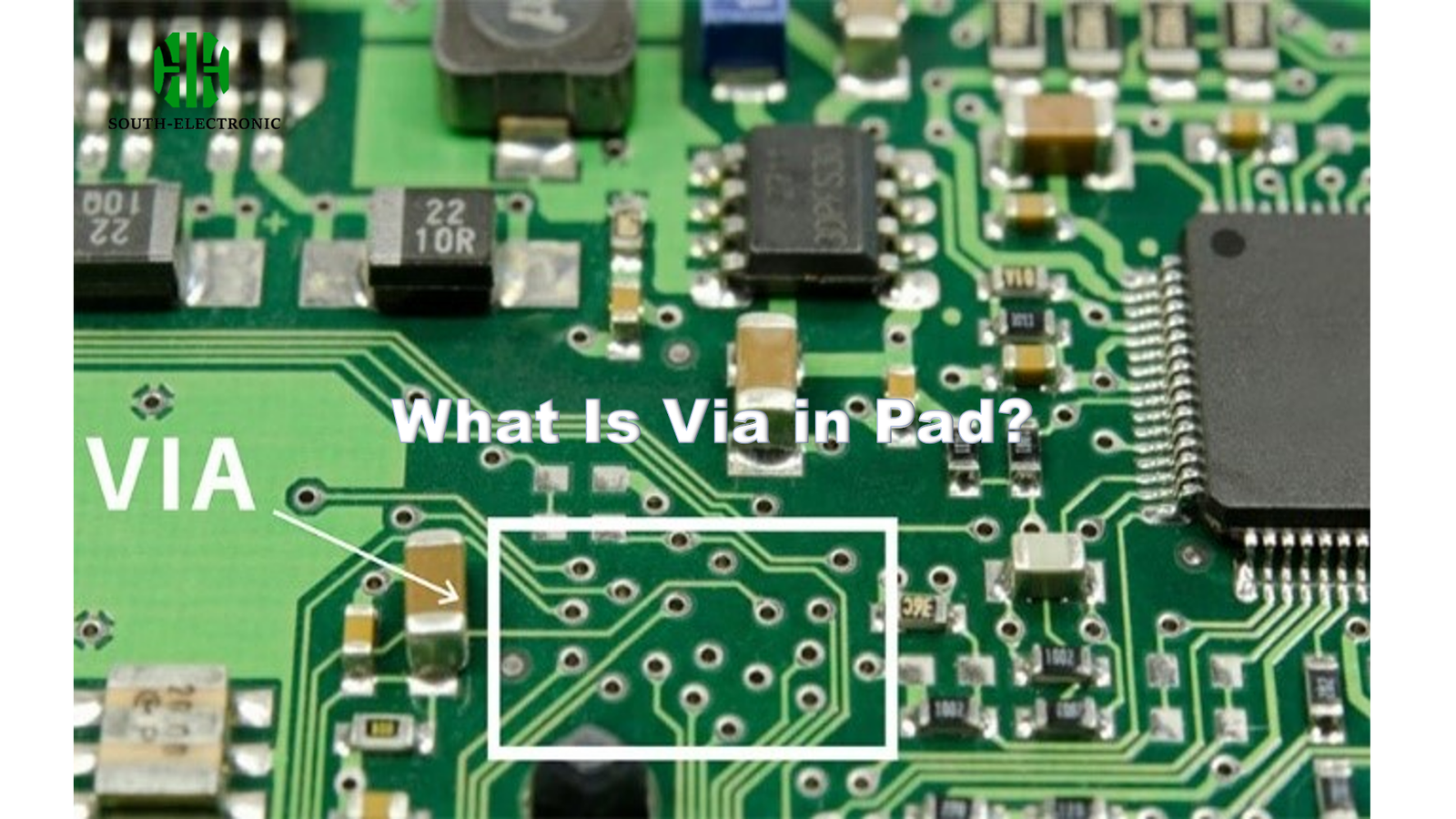
Troubled by cramped PCB designs? Struggling with signal integrity? Via-in-pad might be your solution, but do you truly understand what it is?
Via-in-pad (VIP) is a PCB technology that places vias directly within a component's solder pad. This design eliminates the need for separate routing, connecting layers vertically right at the component pin, saving space and improving performance.
When I first encountered via-in-pad, I was a bit skeptical. Was it just another buzzword, or a real game-changer? It turns out, this clever technique simplifies layouts and boosts performance in ways I hadn't initially considered. Let’s dive deeper into how this works and why it matters for your next project.
What are the advantages of via in pad?
Are you wondering how Via-in-Pad can transform your PCB designs? Many designers face challenges with space constraints and signal quality, making traditional routing a headache.
Via-in-pad offers significant benefits by optimizing space and electrical performance. It creates a direct connection through the pad, which is crucial for modern, high-density designs.

I've seen firsthand how via-in-pad streamlines complex board layouts, especially with fine-pitch components. This method isn't just about fitting more on a board; it's about making those components work better together. The direct connection reduces signal path length, which helps maintain signal integrity. For example, when dealing with high-speed signals, every millimeter of trace length can introduce unwanted impedance and reflections. By placing the via directly under the pad, we minimize these issues. This approach also helps in thermal management, as the via can act as a thermal path, dissipating heat away from components like BGAs.
Space Saving
By integrating the via into the pad, the need for an adjacent 'dog bone' trace is eliminated, freeing up valuable board real estate. This is particularly beneficial for:
- High-density interconnect (HDI) boards: Where component density is extreme.
- Fine-pitch components: Such as BGAs and CSPs, which have very small pad sizes.
Improved Electrical Performance
The direct connection provides a shorter and more direct electrical path, leading to:
- Reduced inductance and capacitance: Enhancing signal integrity for high-frequency applications.
- Better EMI/EMC performance: Minimizing radiation and susceptibility.
- Optimized impedance control: Easier to achieve consistent impedance profiles.
Enhanced Thermal Management
Vias can serve as thermal conduits, transferring heat away from hot spots:
- Thermal vias: Specifically designed to conduct heat from components to ground planes, improving heat dissipation.
- Increased reliability: Preventing component overheating and extending lifespan.
Simplified Routing
Eliminating the need to route traces from pads to offset vias simplifies the overall routing process:
- Cleaner layouts: Less congested board surfaces.
- Faster design cycles: Reduced complexity means quicker routing.
| Feature | Via-in-Pad | Traditional Via |
|---|---|---|
| Space Utilization | High | Moderate |
| Signal Integrity | Excellent | Good |
| Thermal Mgmt. | Excellent | Moderate |
| Routing Complexity | Low | Moderate |
| Cost | Higher (processing) | Lower |
When should I use via in pad?
Are you wondering if via-in-pad is the right choice for your current PCB project? Many designers struggle with deciding when to adopt advanced technologies, fearing added cost or complexity.
You should use via-in-pad when space is at a premium, signal integrity is critical, or thermal management is a concern. It's especially beneficial for complex, high-density, and high-frequency designs.

I've often found myself weighing the pros and cons of implementing via-in-pad. It's not a universal solution, but for certain applications, it’s indispensable. I remember a project where we had a BGA with an extremely tight pitch. Traditional dog-bone routing was simply impossible without adding layers or increasing board size, both of which were unacceptable due to cost and form factor constraints. Via-in-pad was the only viable option, and it saved the design. This technology excels in situations where every square millimeter counts, and where maintaining pristine signal paths is paramount.
High-Density Boards
When dealing with densely packed components and fine-pitch packages like BGAs, CSPs, and QFNs:
- BGAs (Ball Grid Arrays): Via-in-pad allows routing directly through the BGA pads, maximizing routing channels between the balls.
- Miniaturization: Essential for compact devices like smartphones, wearables, and medical implants.
High-Frequency and High-Speed Applications
For designs where signal integrity is paramount, such as:
- RF and Microwave circuits: Minimizing stub length and impedance discontinuities is critical for high-frequency performance.
- DDR memory interfaces: Ensuring clean signal paths for high data rates.
- Gigabit Ethernet and PCIe: Maintaining signal integrity for high-speed digital signals.
Enhanced Thermal Performance Needs
When components generate significant heat that needs to be efficiently dissipated:
- Power components: Vias under power ICs can channel heat to internal ground planes, acting as thermal highways.
- LED arrays: Improving thermal management for high-power LEDs.
EMI/EMC Considerations
For designs requiring strict electromagnetic compatibility:
- Reduced loop areas: Short, direct connections help minimize antenna effects, reducing EMI.
- Improved grounding: Direct connection to ground planes via pads can enhance shielding effectiveness.
Design Complexity Reduction
When struggling with routing congestion and complex layouts:
- Simplified escape routing: Easier to fan out signals from fine-pitch components.
- Fewer layers: In some cases, via-in-pad can help reduce the total number of PCB layers needed, offsetting its higher processing cost.
| Use Case | Benefit Provided by VIP | Example Application |
|---|---|---|
| Space Constraints | Maximizes routing channels | Smartphones, wearables |
| High Frequencies | Improves signal integrity, reduces EMI | RF modules, DDR interfaces |
| Thermal Dissipation | Direct heat path from component | Power converters, LEDs |
| Routing Complexity | Simplifies fan-out from fine-pitch parts | BGA designs, high-pin-count ICs |
Via in pad application for SMD pad?
Are you curious how via-in-pad specifically applies to surface-mount device (SMD) pads? Understanding this can unlock new levels of design efficiency and performance for your SMD components.
Via-in-pad is highly applicable to SMD pads, especially for fine-pitch components like BGAs and QFNs. It allows for direct electrical connection and thermal management within the pad itself, optimizing space and performance.

I've personally found via-in-pad to be a lifesaver when working with various SMD components. It's not just for BGAs; I've used it effectively for smaller QFNs and even some critical passive components where a direct, low-inductance path was essential. The key is understanding that while the concept is simple, its implementation requires careful consideration of manufacturing processes like via filling and capping. When done right, it can significantly improve component reliability and overall board performance. It's about taking the benefits of through-hole vias and applying them strategically to surface-mount technology.
Direct Connection for Fine-Pitch SMDs
For surface-mount devices (SMDs) with very small pad pitches, via-in-pad offers the most efficient way to break out signals:
- BGAs: The most common application, allowing traces to route between the solder balls on internal layers.
- QFNs (Quad Flat No-lead): For thermal pads under QFNs, via-in-pad can create an excellent thermal path to a ground plane.
- LGA (Land Grid Array) and CSP (Chip Scale Package): Similar benefits to BGAs for these compact packages.
Fabrication Process for Via-in-Pad SMDs
Implementing via-in-pad for SMD pads involves specific manufacturing steps:
- Drilling the via: A hole is drilled directly through the SMD pad.
- Plating the via: Copper is deposited to create the electrical connection between layers.
- Via Filling: The via is typically filled with a non-conductive epoxy. This prevents solder wicking into the via during assembly, which could lead to poor solder joints or shorts.
- Via Capping/Plating Over: After filling, the via is capped with copper and plated flat, creating a smooth, planar surface for component soldering. This ensures a reliable solder joint.
Benefits for SMD Assembly
The proper implementation of via-in-pad for SMD pads directly impacts assembly:
- Improved Solder Joint Reliability: A flat, filled, and capped via-in-pad provides a consistent surface for solder paste deposition and reflow, leading to stronger, more reliable solder joints.
- Reduced Solder Bridging: By containing the solder within the pad area, the risk of solder bridging between closely spaced pads is minimized.
- Better Reworkability: Although complex, a well-designed via-in-pad can sometimes make rework processes slightly more manageable compared to highly congested traditional routing.
Considerations for SMD Via-in-Pad
While beneficial, some points need consideration:
- Cost: The filling and capping processes add to manufacturing cost and complexity.
- Design Rules: Strict adherence to manufacturer's design rules is crucial for successful implementation.
- Material Selection: The choice of via fill material can impact thermal performance and reliability.
| SMD Package Type | Primary Benefit of VIP | Key Consideration |
|---|---|---|
| BGA | Maximized routing density | Via fill & cap |
| QFN | Enhanced thermal dissipation | Thermal pad connection |
| CSP | Miniaturization, signal integrity | Fine pitch design |
| LGA | Reliable electrical connection | Planarity |
Conclusion
Via-in-pad is a powerful PCB technology offering space savings, improved electrical performance, and better thermal management. It's a key technique for modern, high-density electronics, making it essential for current and future designs.

