
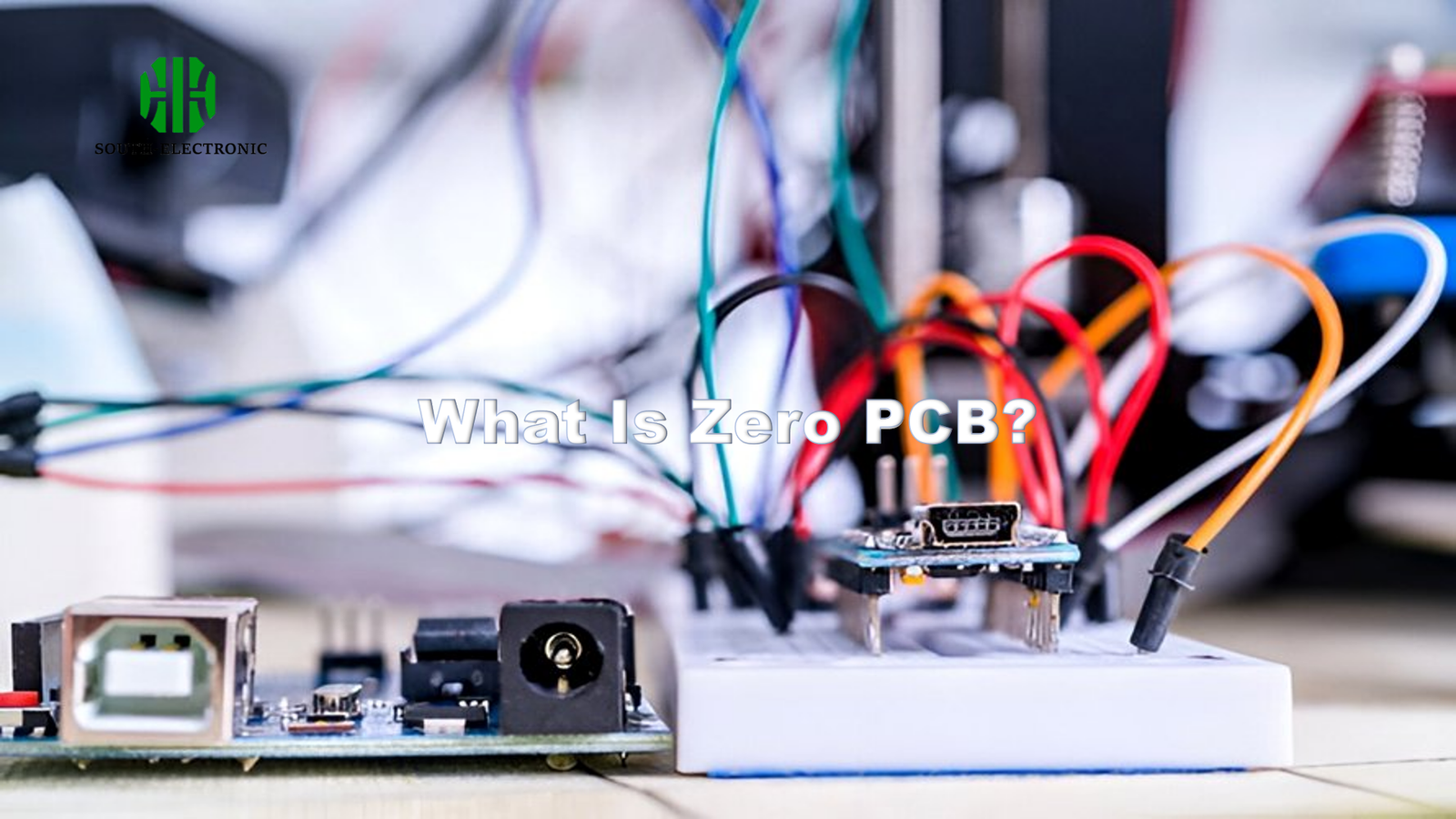
Ever struggled to prototype circuits without custom PCBs? Zero PCB solves this dilemma. This versatile board lets you create instant circuits without etching or complex designs. Keep reading to unlock its full potential.
Zero PCB is a universal copper board with holes spaced 2.54mm apart, used for prototyping. Unlike custom PCBs, it requires no etching, letting you build circuits by directly soldering components through pre-drilled pads.
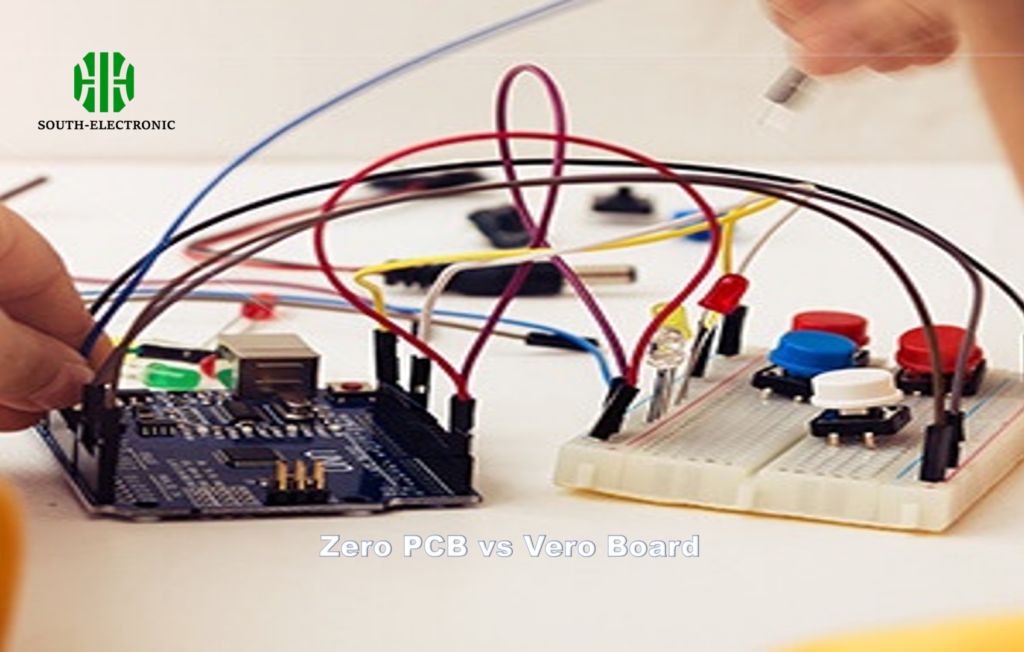
If you think this sounds similar to Vero boards, you’re half right. Let’s break down the unique advantages and limitations to help you choose the right platform for your next DIY project.
Zero PCB vs. Vero Board
Confused between Zero PCB[^1] and Vero Board[^2]? The right choice depends on your specific needs. Both allow quick prototyping but have critical differences in functionality.
Choose Zero PCB for soldering through-hole components in custom layouts. Opt for Vero Board for surface-mount parts and preset connection patterns. Zero PCB offers full design freedom, while Vero Board simplifies repeat circuits.
Key Comparison Factors
| Factor | Zero PCB | Vero Board |
|---|---|---|
| Structure | Isolated copper pads | Pre-connected copper strips |
| Components | Through-hole preferred | Surface-mount friendly |
| Modifications | Easy cut traces | Fixed connections |
| Cost | ₹50-₹150 | ₹80-₹200 |
| Best For | One-off prototypes | Repeated circuit designs |
Zero PCBs work best when each connection needs customization. I once burned three Vero Boards trying to modify a sensor circuit before switching to Zero PCB. The isolated pads let me reroute wires without damaging adjacent components. However, Vero Boards save time for common amplifier circuits where preset copper strips match the required connections.
How to Build a Circuit Using Zero PCB: Step-by-Step Guide
New to Zero PCB? Don’t worry. Building your first circuit requires just five tools and basic soldering skills.
1. Place components on pads. 2. Solder joints. 3. Connect related points with wires. Use side cutters to trim excess leads. Test continuity before powering.

Essential Tools & Tips
| Tool | Purpose | Pro Tip |
|---|---|---|
| 25W Soldering Iron | Component soldering | Keep tip clean for better heat transfer |
| Lead-Free Solder | Creating joints | Use 0.8mm thickness for precision |
| Wire Cutter | Trimming component legs | Cut at 45° angle to prevent short circuits |
| Multimeter | Testing connections | Check resistance between adjacent pads |
| Jumper Wires | Bridging non-adjacent pads | Use 24AWG wires for low-current circuits |
Always start from the center and work outward. I ruined my first Zero PCB by soldering[^3] edge components first, causing warping. For ICs, use a DIP socket—desoldering chips from these boards often damages copper pads.
What Projects Are Best Suited for Zero PCB vs Standard PCB?
Choosing between Zero and standard PCBs? Your project’s scale and complexity will decide.
Use Zero PCB for prototypes/testing (under 10 units). Switch to standard PCBs for final products needing durability, compactness, or complex multilayer circuits.
Project Match Guide
| Requirement | Zero PCB | Standard PCB |
|---|---|---|
| Quantity | 1-10 units | 50+ units |
| Turnaround Time | Immediate | 5-14 days |
| Complexity | Single-layer designs | Multi-layer circuits |
| Cost Efficiency | ₹10/unit (material only) | ₹2/unit (bulk orders) |
| Modifications | Easy | Requires new fabrication |
I learned this the hard way after using Zero PCBs for 30 WiFi sensors. While affordable initially, reassembling each unit took 3× longer compared to manufactured PCBs. Now I reserve Zero PCBs for proof-of-concept builds and first-stage testing.
Conclusion
Zero PCB excels for DIY prototyping with instant usability. Match it with Vero Board for repetitive designs, and switch to standard PCBs for mass production. Choose wisely based on your project phase and complexity needs.
[^1]: Explore this link to understand the innovative features of Zero PCB and how it can enhance your prototyping experience.
[^2]: Discover the benefits of Vero Board for circuit design, especially for surface-mount components and repeatable layouts.
[^3]: Discover effective soldering techniques that can improve your skills and ensure better connections in your projects.

