
What are the differences between FPC and PCB?

Flexible PCBs enabling bendable, lightweight designs for smartphones, wearables & drones. Offer thinness, high density, & durability vs rigid PCBs. Future driven by innovation.
Why do PCB warp?

PCB warping causes assembly errors, machine damage, & post-solder defects. Driven by material CTE mismatches, uneven copper, lamination issues & stress. Prevention requires design symmetry, material control, specific lamination techniques & post-bake processes.
Is PCB “edge wrapping” important?

PCB edge wrapping adds protective plating/coating to board borders. Prevents corrosion, boosts mechanical strength, enhances solderability, improves EMI shielding & extends lifespan. Vital for reliability.
What problems can occur with PCB soldering?

Common PCB soldering problems (open circuits, shorts, cold joints, etc.): causes include wrong parameters, equipment, materials, technique, & design defects. Solutions provided.
How much do you know about single-sided aluminum PCBs?

Aluminum PCBs excel in heat dissipation for high-power electronics via metal-core structure (circuit, dielectric, aluminum base), offering efficient cooling, insulation, and cost-effective machinability.
What are the top-tier PCB and hardware designs for the iPhone 17?

Explore the iPhone 17 series: 17, Pro, Pro Max, and ultra-thin iPhone Air. Features A19 chips, OLED screens, and camera upgrades. Pro models boast removable midframes for easier battery swaps and vapor chamber cooling.
What common PCB terminology do you know?

Detailed guide explaining 25 essential PCB terms like annular ring, DRC, gold fingers, reflow soldering, vias, solder mask, and manufacturing processes.
Do you know PCBs? A beginner’s guide

Trace PCB evolution from point-to-point wiring, explore their layered structure (base material, copper, solder mask, silkscreen), assembly basics, and key terminology driving modern electronics design.
Master PCB Stackup Design Tips in One Article

Learn PCB stackup design principles (adjacent ground layers, symmetry) for optimal impedance matching in high-speed circuits. Includes RK3588 8-layer through-hole case study with trace width calculations using DFM tools.
What are the causes of uneven color in PCB manufacturing?
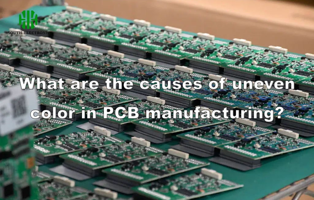
Learn 11 causes of uneven PCB color like squeegee blade issues, improper ink viscosity, screen gap problems & printing speed. Discover fixes for consistent PCB appearance.
