
What is a Molex Connector?

Early PCB warpage testing saves costs. Mild warps can be reworked; severe cases need scrapping. Prevent warpage via balanced copper, low-CTE materials & controlled lamination. Flatness ensures perfect assembly.
What are the design rules and best practices for power planes?

Master PCB power planes with dedicated layers, optimal copper thickness, strategic splits for multiple voltages, and decoupling placement. Prevent overheating, noise, and failures in critical designs.
What are the key components in a vape circuit?

Understand vape circuit components to fix failures. Learn how to choose certified PCB manufacturers, optimize performance for vapor/battery life, and verify safety certifications.
What is PCB Mount?

Learn PCB mounting essentials: secure components with pillars, choose stabilizers, place holes properly. Prevent failures and ensure electronics stability through correct mounting techniques.
How to choose the right PCB pin?

Choose reliable PCB pins: match material to environment, ensure precise fit/strength, and test rigorously to prevent signal loss, solder failures, and costly device breakdowns.
How to convert hand-drawn PCB ideas to Gerber files?
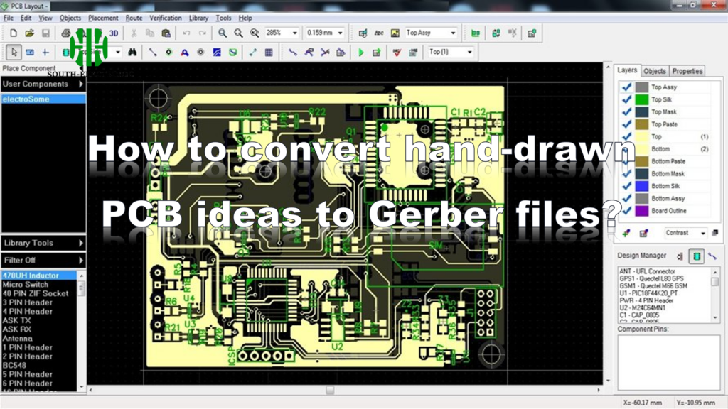
Master converting hand-drawn PCBs to Gerbers in Altium/Cadence! Learn scanning, component placement, power/signal routing rules, noise reduction, and creative layout techniques.
What is ESP32, and why is it popular?
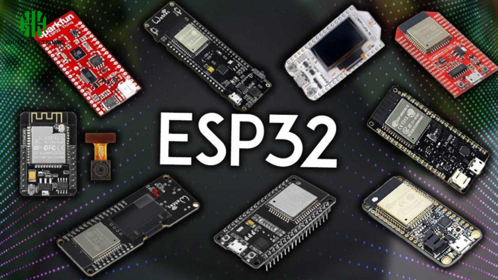
Unlock big IoT potential with tiny, budget-friendly ESP32 chips! Master board selection, setup in minutes, fix common issues, and outshine Raspberry Pi for low-power projects. Start now.
Which IC packages dominate modern electronics?
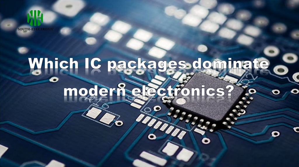
Master IC package selection: BGA for high-speed/high-pin, QFP for cost efficiency. Unlock chiplet/3D performance gains and conquer signal/thermal challenges with proven PCB strategies.
What is BGA soldering?
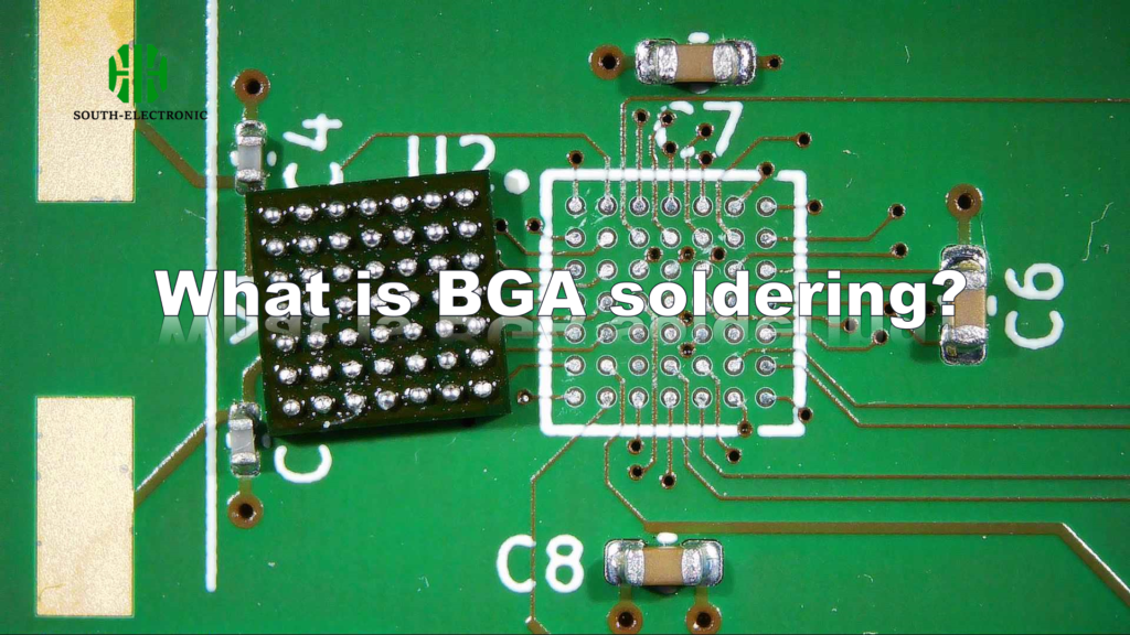
Master BGA soldering: Prevent bridging/voids with precise temp control, baking & flux. Essential tools: stencils, reflow ovens, X-ray inspection ensure reliable high-density connections.
What is a blind via?
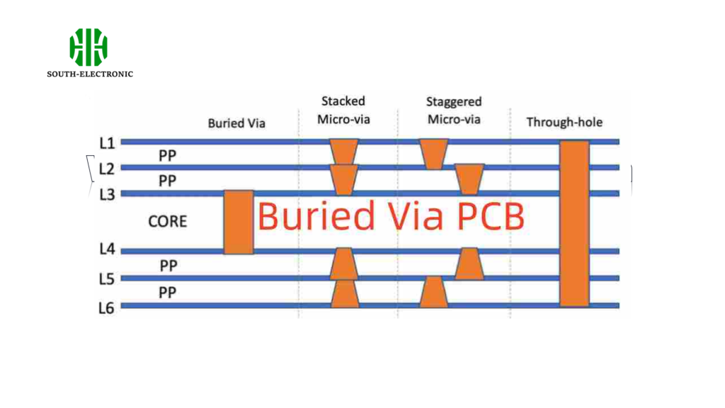
Blind vias save space in dense PCBs by connecting outer to inner layers selectively. Essential for HDI designs like smartphones, they optimize routing & thermal management, but increase cost 15-30%. Combines with microvias.
