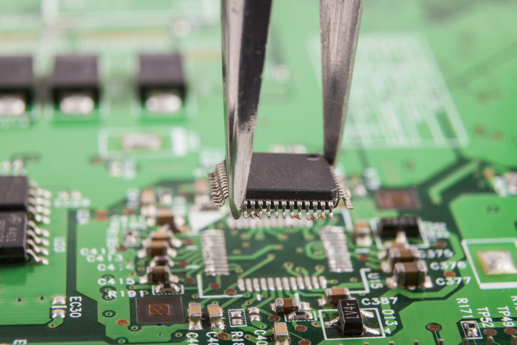
Find the golden rule in Layout!

Top 10 PCB design rules for optimal layout and manufacturing: grid selection, routing, power planes, component grouping, panelization, DRC, silkscreen, capacitors. Boost reliability and cut costs.
Why Avoid Human Inspectors in PCB Assembly?

Automated optical inspection (AOI) cuts PCB errors by 95% vs manual checks. Learn AOI vs SPI vs AXI cost/ROI comparisons, false alarm fixes, and key supplier selection criteria.
What is a Plated Through Hole?
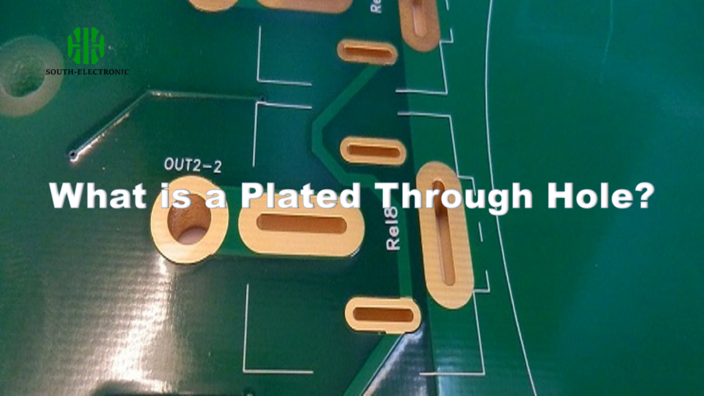
Plated Through Hole (PTH) technology uses copper-lined holes to create reliable electrical connections between PCB layers, preventing signal failures & strengthening component mounts. Vital for complex electronics.
How to Clean a PCB by Hand Without Damaging Components?
Safely clean PCBs without damage using manual brushing with isopropyl alcohol, distilled water rinsing, and thorough drying. Avoid ultrasonic risks targeting corrosion and residues.
What is silver solder?
Prevent electronics solder joint failures! Silver solder creates robust metallurgical bonds for aerospace, medical & military PCBs. Master techniques, inspection & material selection.
What Frequency Range Qualifies as “High Frequency” for PCBs?

Master high-frequency PCB design: Why FR4 fails above 500MHz, material selection impact (Dk/Df), lamination precision, and RF-specialized manufacturing prevent signal chaos. Key for GHz success.
Where to Get Cheap and Reliable Custom PCBs?

Get affordable custom PCBs from verified Chinese manufacturers. Avoid costly design mistakes and assembly pitfalls with proven DFM checks and testing protocols. Start saving now!
What are the Essential Layers in a PCB?

Essential PCB layers: substrate, copper, solder mask, silkscreen. Optimize stack-up with thickness choices (copper/dielectric), 4 vs 6-layer tradeoffs, and signal integrity fixes for reliable boards.
Why Do PCB Resistors Overheat?
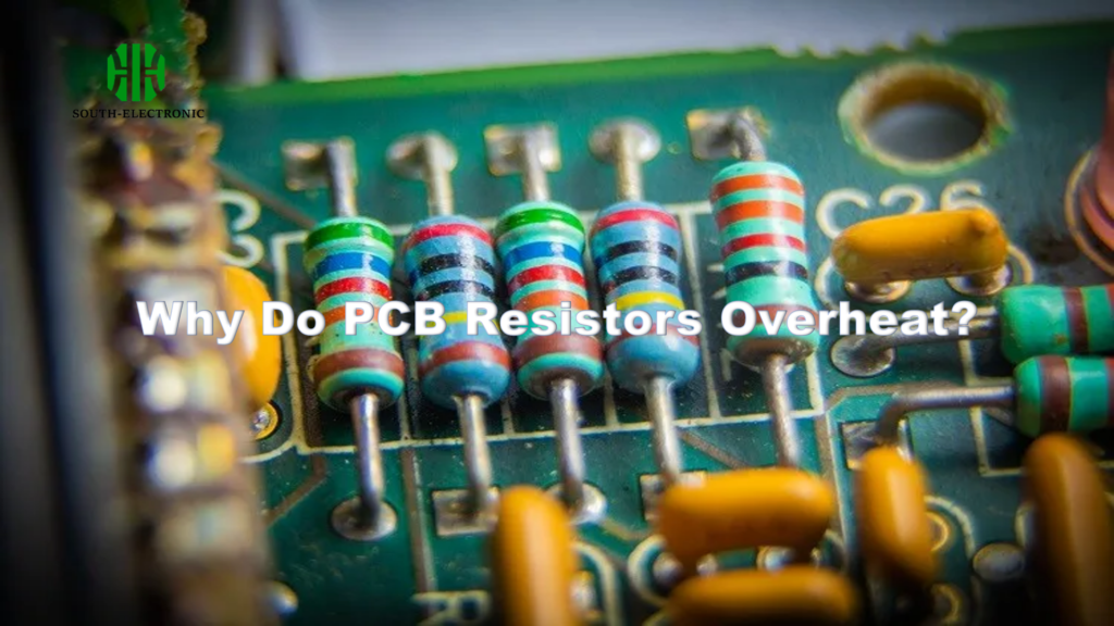
Prevent PCB resistor overheating: accurately calculate power, ensure thermal design/footprint, choose 2x rated resistors & embedded for high-speed. Test early, avoid failures.
How to Choose Between Board-to-Board vs. Wire-to-Board Connectors?
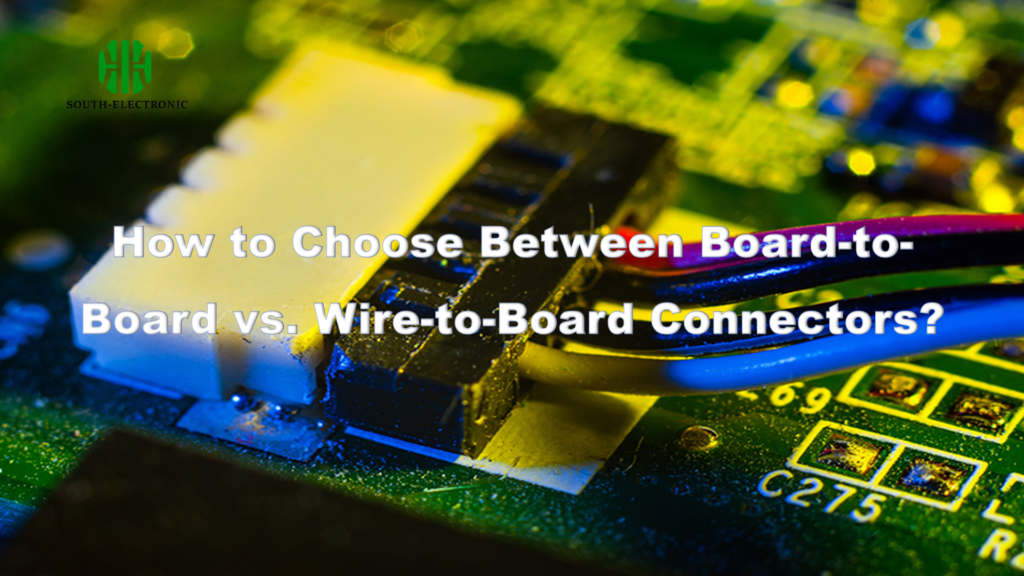
Select board-to-board or wire-to-board connectors based on link type/space constraints. Solve density via pin pitch/current ratings, vibration with cage clamps, and optimize Molex use. Prevent failures via validation.