
What is AOI in PCB?

AOI systems detect PCB defects with 99.9% accuracy using ML and high-res cameras, preventing costly recalls and ensuring manufacturing compliance.
What is Optical PCB?
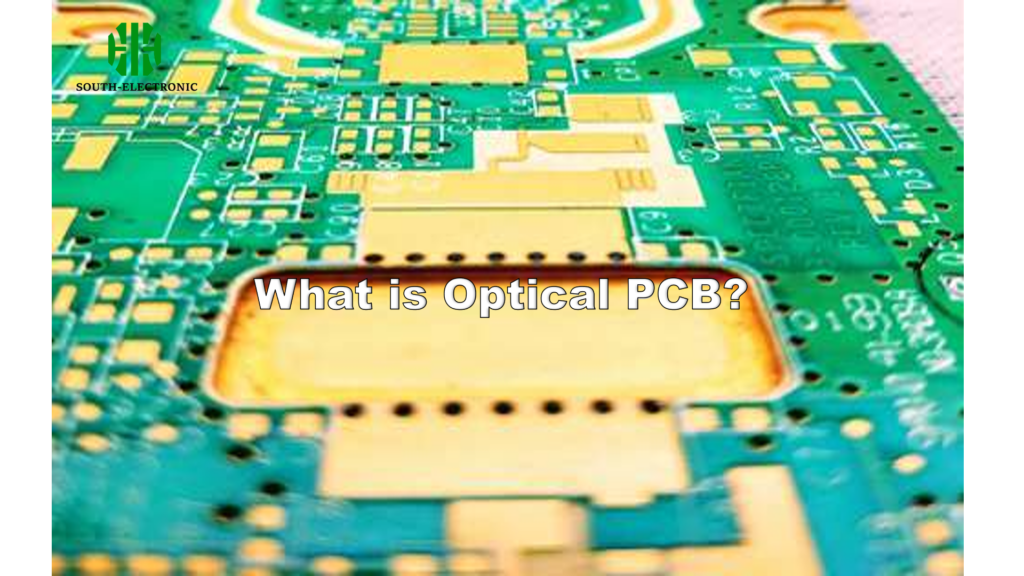
This article delves into the intricacies of PCB optical modules, discussing their applications, technical requirements, distinct characteristics, and key process controls. The aim is to shed light on how these components are changing the technological landscape and the critical factors that drive their efficiency and reliability.
Do you know the knowledge of PCB crystal oscillator?
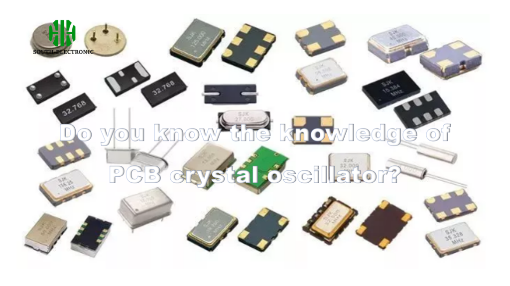
Crystal oscillators, vital in electronics, include active (with IC) and passive types. Key PCB design tips: placement, proximity, short wiring, grounding, and isolation for stability.
How to Reverse Engineer a PCB?

PCB reverse engineering guide: Step-by-step process to decode legacy boards using software tools, layer analysis, legal compliance, and rigorous validation.
What is the PCB Electroplating Hole Filling Process?

PCB via electroplating prevents signal loss & overheating – learn conductive vs non-conductive fillers, thermal management, & defect solutions.
How to draw PCB without understanding EMC?
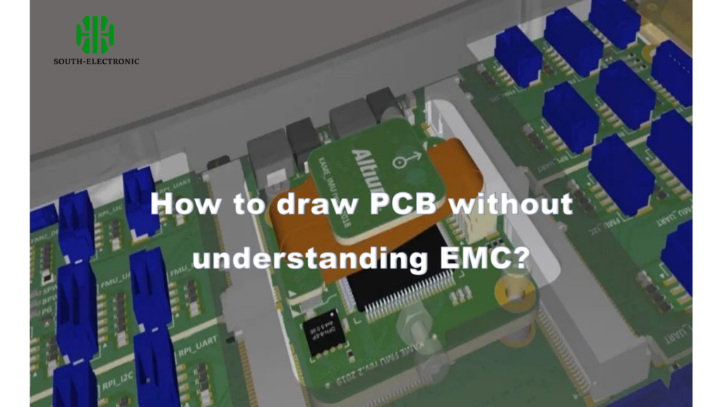
Learn EMC PCB design strategies for EMI reduction: optimize layering to minimize return paths, strategic component layout, & signal routing rules for enhanced EMI suppression.
How Does Laser Drilling Work in PCBs?
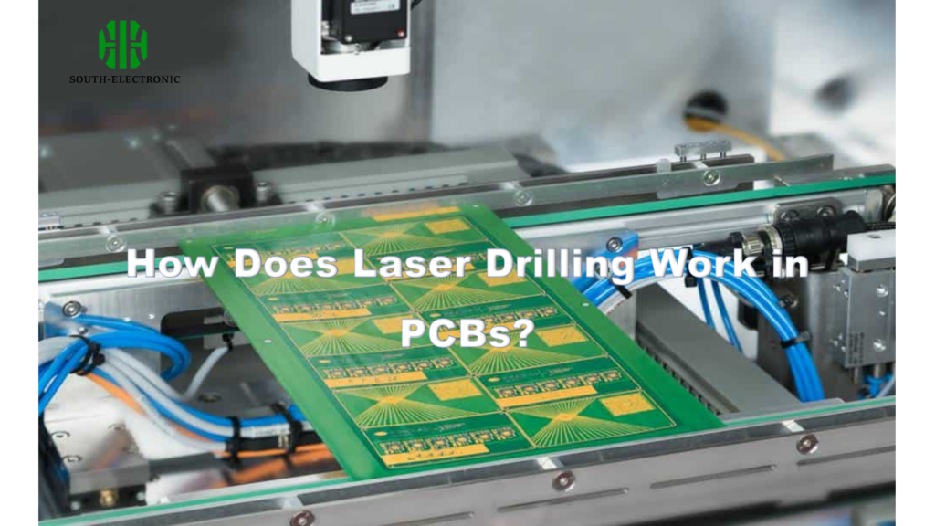
Laser drilling enables ultra-precise microvias for HDI PCBs and 5G devices, offering superior accuracy, cost-efficiency, and reliability in modern tech.
What is the BGA Package?
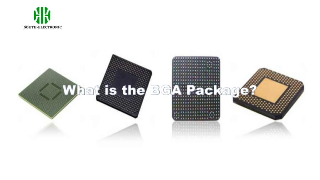
BGA packages enable compact, high-performance electronics via dense solder ball arrays. Key for modern PCB designs in smartphones, automotive, IoT, and aerospace tech.
What Is the Role of Three-Proof Varnish in PCB?

Three-proof varnish shields PCBs from extreme heat, moisture, and corrosion, ensuring reliability in automotive, aerospace, and marine electronics.
What Is the Difference Between PCBA and PCB?
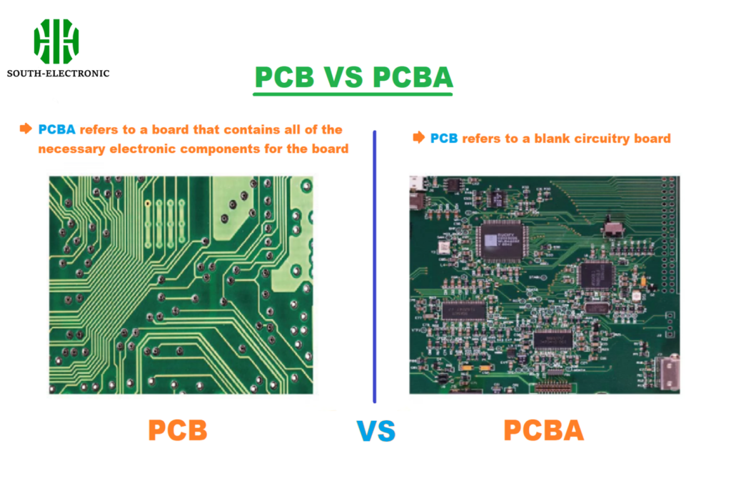
PCB vs PCBA explained: avoid costly mix-ups. Learn critical differences in manufacturing, testing, and budgeting for efficient electronics production.
