
What Should Be Paid Attention to During PCB Proofing?

Master PCB proofing with design checks, cost control, advanced tools, and supplier partnerships to eliminate prototyping failures.
How to Make a High-Quality Circuit Board?

High-quality PCBs use photolithography, lamination, plating vs. traditional student etching. Enables multi-layer boards, <4 mil pitches, reliability. Critical: testing, thermal/signal integrity, eco-friendly processes.
What is Conformal Coating for PCB?

Conformal coatings protect PCBs from moisture, dust, and heat with materials like silicone/acrylic. Critical in automotive, aerospace, and medical tech. Emerging trends include self-healing coatings.
What is PCB Back Drilling?
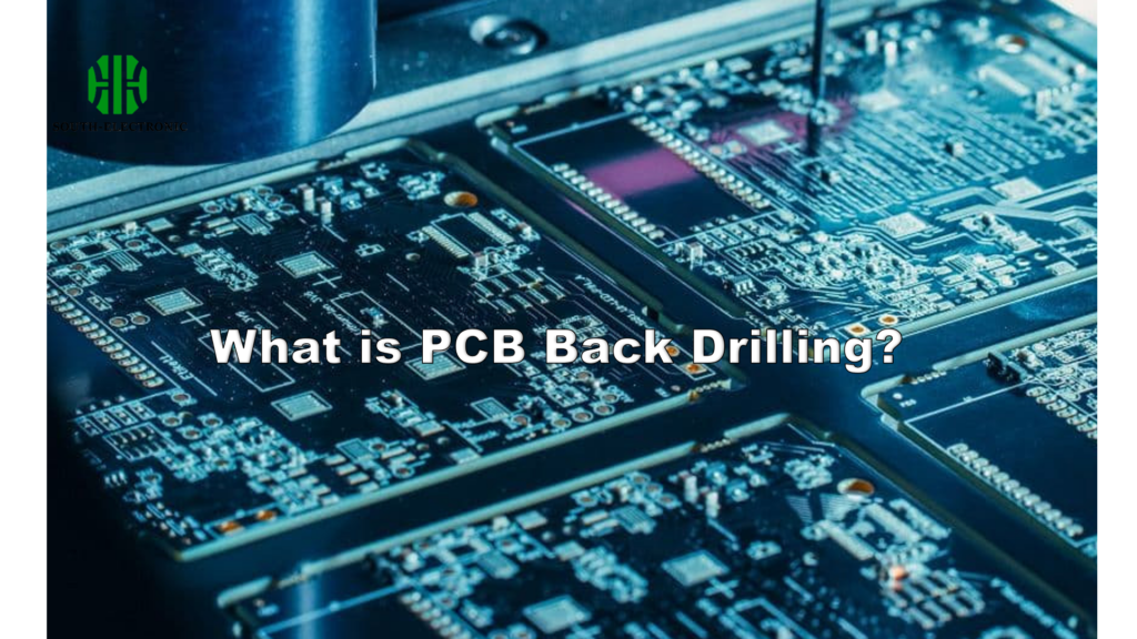
PCB back drilling removes copper stubs in vias, optimizing high-frequency signal integrity for 5G, AI, and aerospace electronics.
What is Reflow Soldering?

Master reflow soldering stages, thermal profiling, and defect prevention techniques for military, automotive, and IoT/5G electronics reliability.
What is a Multilayer PCB?
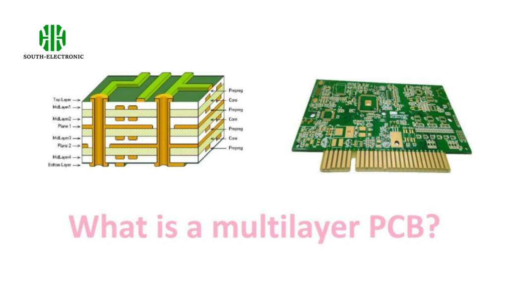
Multilayer PCBs stack copper/dielectric layers, enabling compact, high-speed electronics – the backbone of smartphones, medical devices, and 5G tech.
Why Nitrogen is Essential for PCB Assembly?
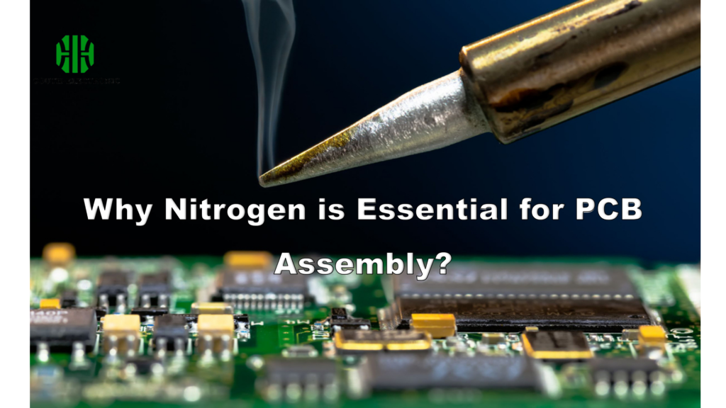
Nitrogen soldering slashes defects 40-70% by eliminating oxidation. Crucial for modern PCBs—explore benefits, chemistry, ROI for all scales
What is DNP in PCB Design?
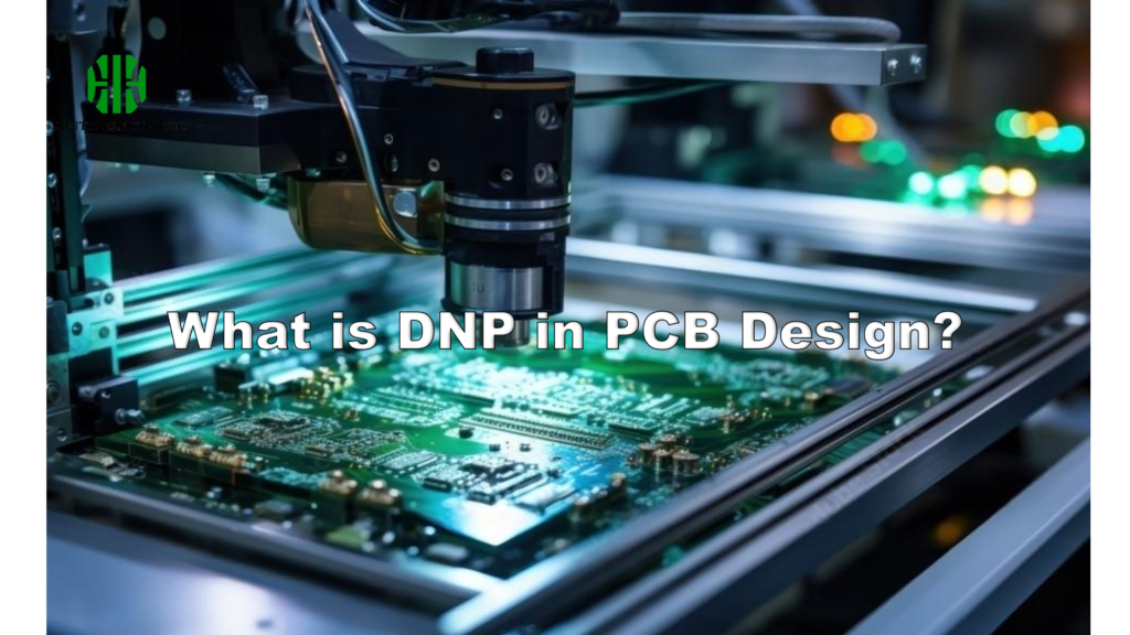
Master DNP markers in PCB design to prevent costly assembly errors, ensure BOM accuracy, and save costs with silkscreen/BOM best practices.
What is High Frequency PCB?
This article delves into High Frequency PCBs, highlighting their advanced materials, intricate design, and pivotal role in modern electronics. It explores their manufacturing, design considerations, and applications, emphasizing their significance and evolving impact in technology, from communication systems to AI integration.
Why Do PCB Manufacturing Processes Produce Ink Bubbles?
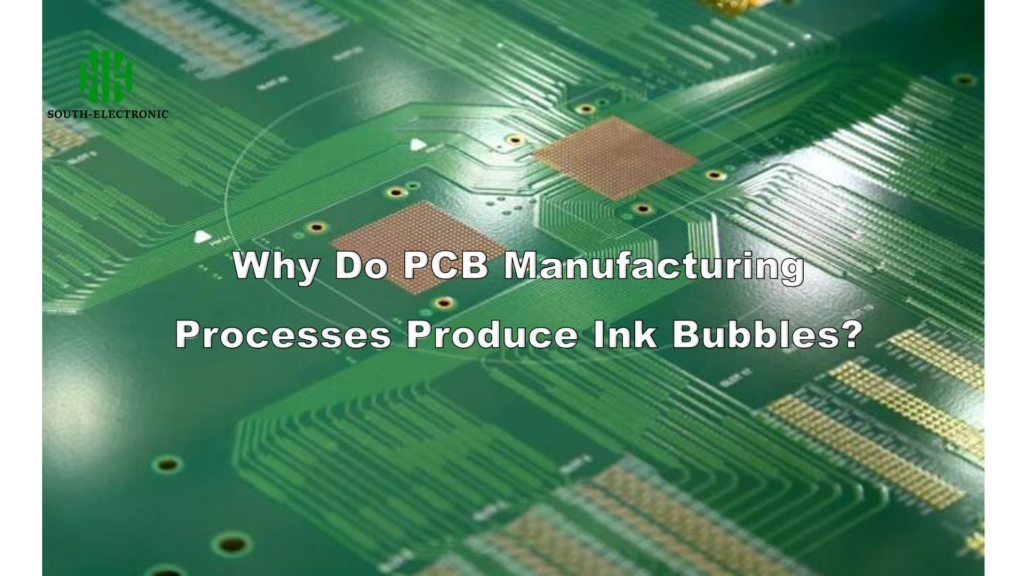
Ink bubbles in PCBs stem from material mismatches, process errors, contamination, and humidity. Solutions: surface engineering, process controls, nano-materials, μCT inspection.
