
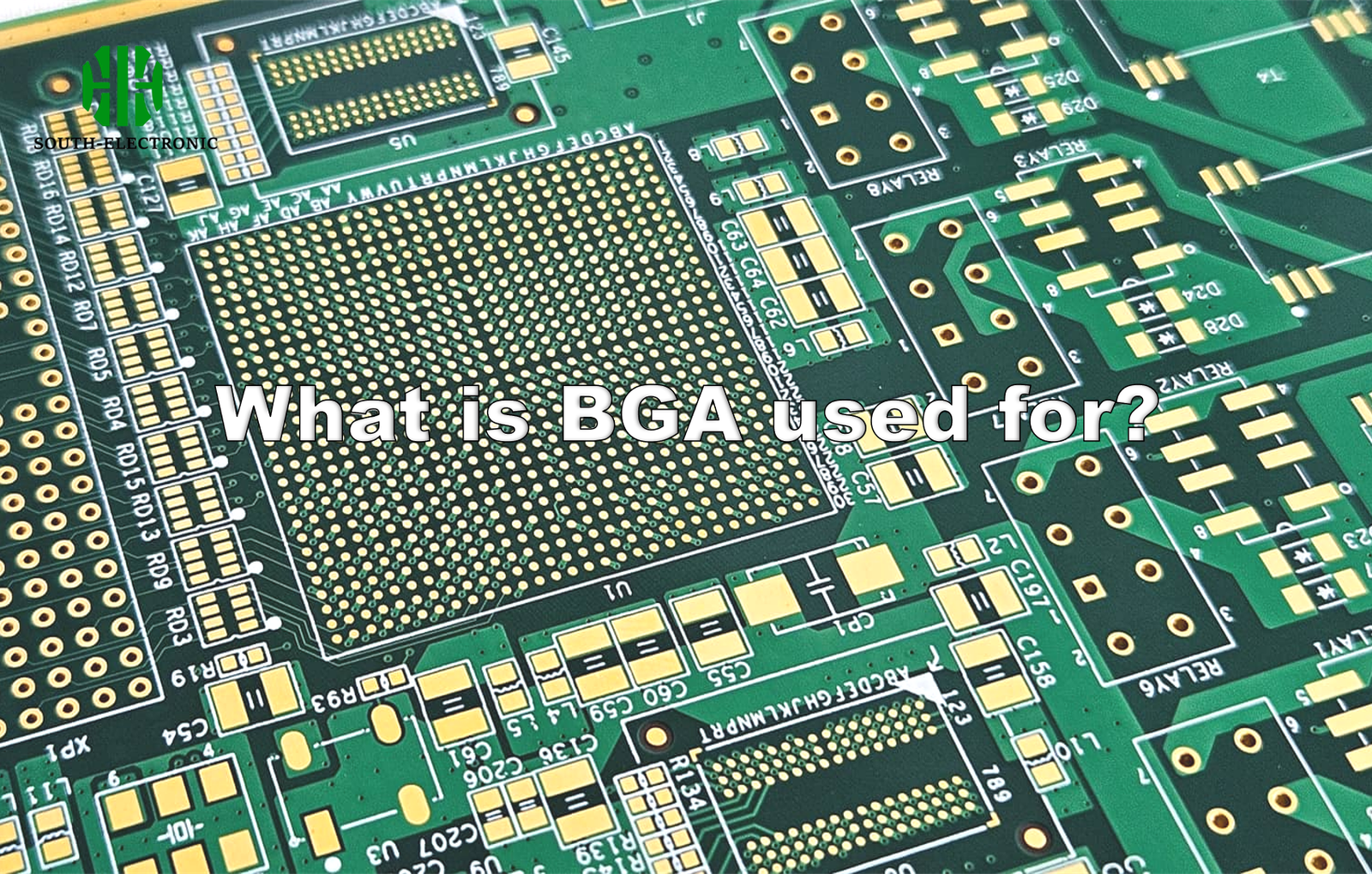
Ever struggled with circuit board failures in your smartphone? Frustrated by overheating processors or flaky connections? BGA packaging[^1] solves these modern electronics nightmares.
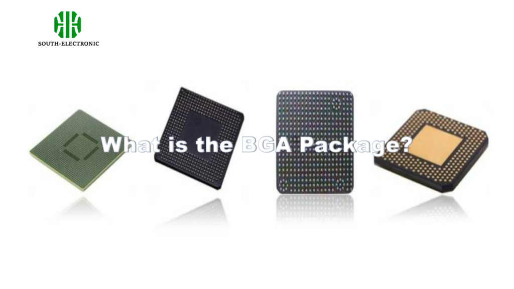
BGA (Ball Grid Array) packs solder balls under ICs for processors, GPUs, and memory where performance matters most. Its dense layout beats old pin designs, boosting electrical flow and cooling for phones, computers, and telecom devices using tight spaces or high power.
Understanding BGA unlocks smarter designs. Now let’s explore key design rules, repair realities, and alternative package comparisons for your next project.
What are the key design points for BGA PCB?
Watch your board fail from thermal stress? Tiny BGAs demand precision planning many overlook starting out.
Focus on pad alignment, trace routing, and thermal vias[^2]. Perfect pad size prevents solder bridges while escape routing avoids signal interference like crosstalk or noise.
Critical Design Elements Broken Down
Success hinges on three measurable factors:
| Element | Why It Matters | Best Practice |
|---|---|---|
| Pad Diameter | Prevents ball overlaps | Match ball size ±10% |
| Via Placement | Avoids drilling damage | Use micro-vias outside pads |
| Laminate Choice | Controls heat dissipation | Select low-CTE laminates |
High-density boards need controlled impedance traces[^3]. I prefer 45° dog-leg routing between balls which lowers capacitance versus 90° turns. For thermal demands, stagger via patterns under chips using filled vias—this drops junction temps by 15°C in stress tests. pcb laminate thickness[^4] becomes critical here; thicker cores like 2.4mm help with warping during reflow. Always simulate thermal expansion early: copper density changes impact pcb laminate material stability across temperature cycles. Balance requires considering pcb laminate vs prepreg ratios too—I’ve seen 70% resin content laminates prevent layer separation at peak reflow temps.
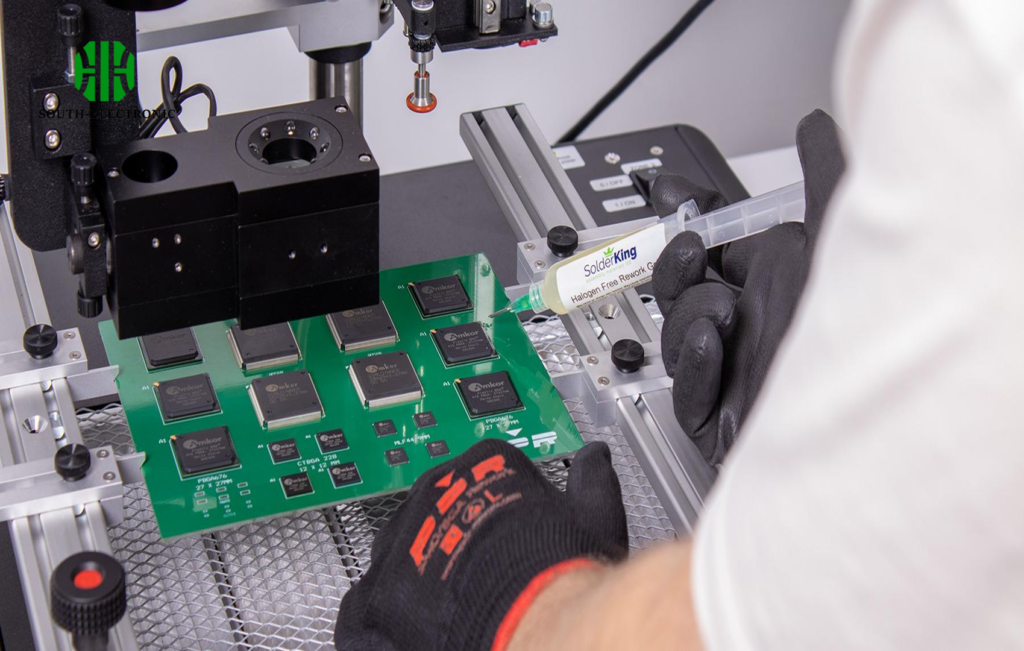
Can You Really Rework a BGA Component?
Faced a $500 board scrap because one chip failed? Many engineers wrongly assume BGAs are disposable after soldering.
Yes, professional rework succeeds with infrared heaters and precision tooling. Accurate temperature profiling preserves the board while melting solder balls cleanly underneath.

Step-by-Step Rework Reality Check
The key phases involve controlled heating and microscopes:
| Stage | Equipment Needed | Risk Factor |
|---|---|---|
| Removal | Hot air nozzle | Pad lifting |
| Site Cleaning | Copper braid wick | Overheating damage |
| Alignment | Optical centering tool | Ball misplacement |
I’ve salvaged 0.4mm-pitch BGAs using temperature ramps of 3°C/second—faster rates crack adjoining components. pcb laminate manufacturing process[^5] choices determine survival odds; low-loss materials like FR4-TG170 maintain pad adhesion during reheats. When sourcing kits, reliable pcb laminate manufacturers in india like Ventec offer halogen-free versions resisting delamination. Crucially, prepreg flow rates impact layer bonding—higher resin viscosity minimizes blistering below chips. Remember: component reuse depends on pcb laminate types handling repeated 260°C reflow peaks without discoloration.
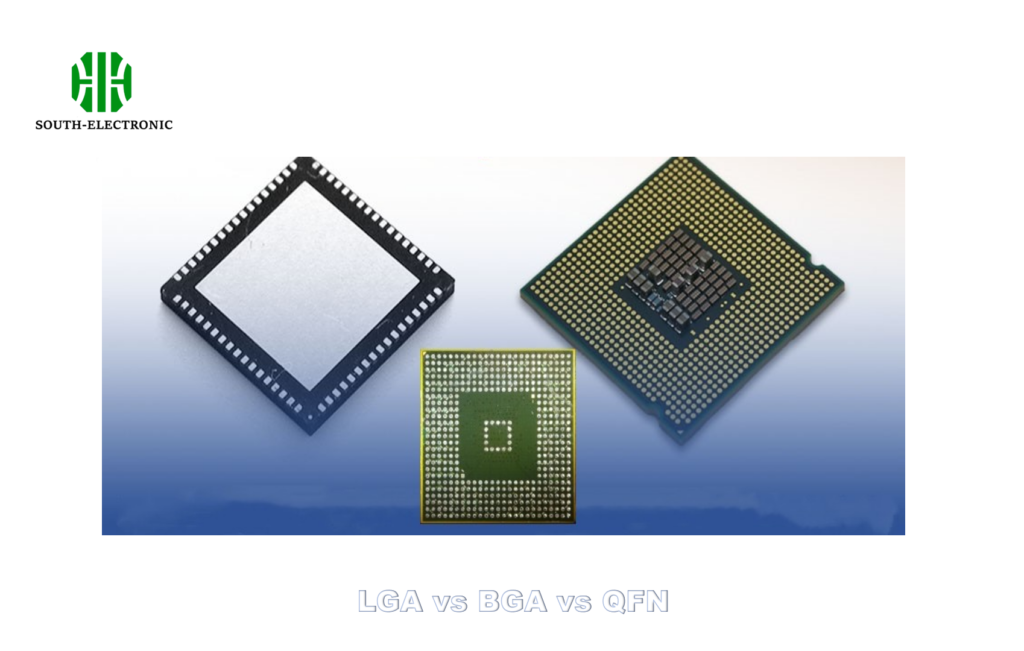
BGA vs. QFN vs. LGA: How to Choose the Right Package for Your PCB Board?
Stuck parsing packaging datasheets? Each IC format fits different price-performance niches you can’t ignore.
Select BGA for maximum pins under 20mm², QFN when cost rules, or LGA for sockets needing swaps. Balance pin density against thermal sinks and assembly costs per design phase.
Decision Matrix for Real Projects
The choice pivots on your board constraints:
| Package | Pin Density | Rework Difficulty | Thermal Performance |
|---|---|---|---|
| BGA | ★★★★★ | ★★★★ | ★★★★★ |
| QFN | ★★★☆☆ | ★★☆☆ | ★★★★☆ |
| LGA | ★★★★☆ | ★☆☆☆ | ★★★☆☆ |
pcb laminate manufacturers like Isola shine for BGAs needing stable heat removal—their RF laminates star in 5G modules. Conversely, QFNs pair well with thin cores; aim for pcb laminate thickness below 1.6mm if manual soldering. I avoid LGAs on multi-layer boards because spring contacts demand flatter surfaces than most pcb laminate material grades provide. Mid-project switches? Check pcb laminate vs prepreg Td (decomposition temp)—some bargain laminates scorch above 200°C during LGA socket soldering. Always prototype with your planned pcb laminate manufacturing process to catch warping early.
Conclusion
BGA enables smaller, faster electronics but demands precise design and rework skill. Match its strengths to high-performance needs after comparing packages thoroughly.
[^1]: Explore this link to understand how BGA packaging enhances performance in modern electronics.
[^2]: Understand the role of thermal vias in managing heat dissipation in circuit boards.
[^3]: Explore the significance of controlled impedance traces for signal integrity in high-speed designs.
[^4]: Learn about the importance of PCB laminate thickness for preventing warping and ensuring reliability.
[^5]: Gain insights into the PCB laminate manufacturing process to ensure quality and performance.

