
What Are the Key Processes in Double-Sided FPC Manufacturing?
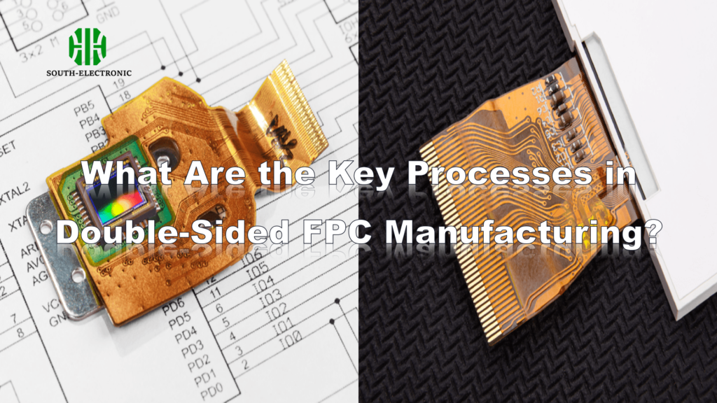
Discover key double-sided FPC steps: cutting, drilling, hole metallization, cleaning & resist coating. Learn how precision ensures flexible circuit reliability.
What should be paid attention to in PCB power supply layout?
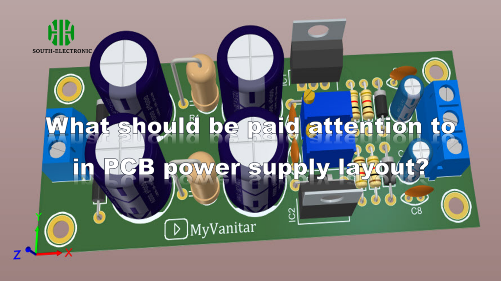
Critical PCB layout practices for buck converters: minimize high-di/dt power loop area with short/thick traces, place input caps near Vin/PGND, reduce SW noise impact, and optimize copper/vias for thermal/EMI performance. Essential for stable power delivery.
How to Design the Perfect BGA?

Master BGA design: Avoid routing nightmares, thermal chaos & hidden defects with IPC standards, microvia strategies, thermal management, rework, and advanced QA.
Why Are Ceramic PCBs More Expensive?
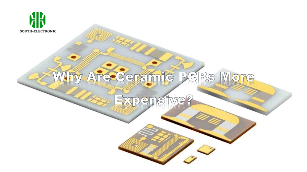
Why choose costly ceramic PCBs over FR4? Essential for >150°C/high-frequency applications with unmatched thermal conductivity & signal integrity. Avoids system failures despite higher cost.
How to Realistically Shortlist Your Ideal China PCB Manufacturer?

Avoid China PCB partner pitfalls: demand full cost transparency, validate Gerber files rigorously & cultivate multi-site resilience. Prioritize technical skill over lowest price.
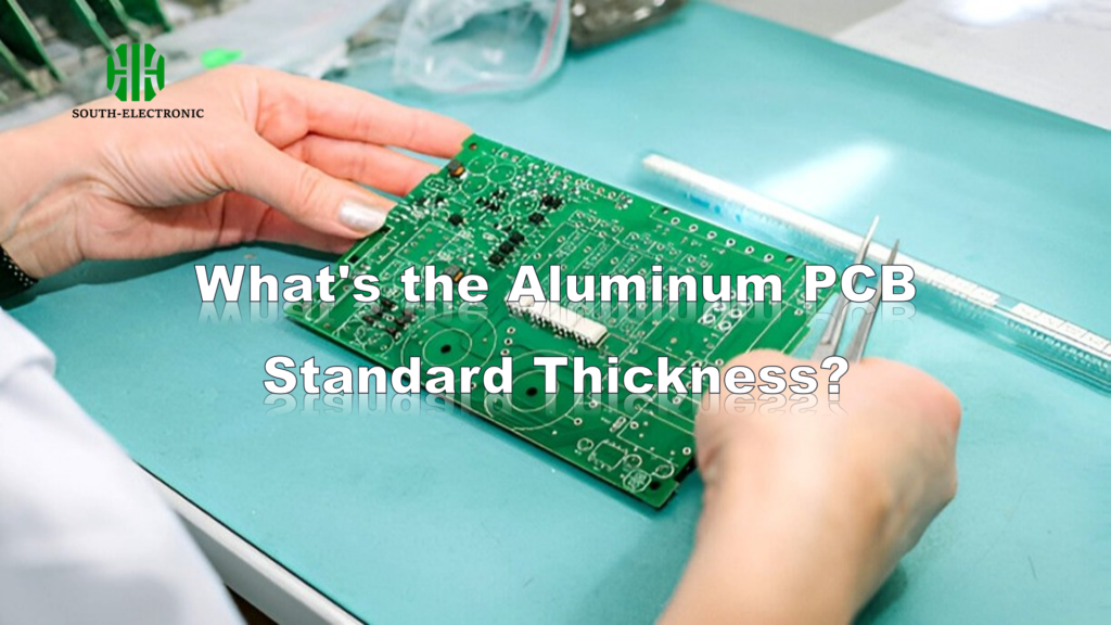
What’s the Aluminum PCB Standard Thickness?
Choose LGA over BGA for cheaper repairs, easier visual inspection & thermal efficiency. Ideal for desktops/servers needing upgrades without performance loss. Cut manufacturing costs & downtime.
When choose LGA over BGA?
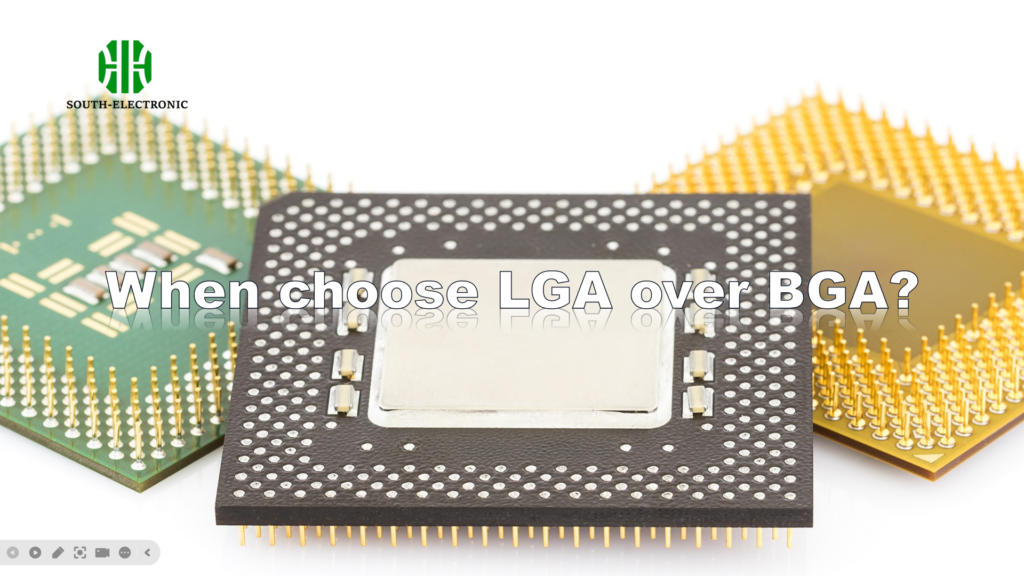
Choose LGA over BGA for cheaper repairs, easier visual inspection & thermal efficiency. Ideal for desktops/servers needing upgrades without performance loss. Cut manufacturing costs & downtime.
Can Free PCB Layout Software Truly Challenge Altium or Eagle?
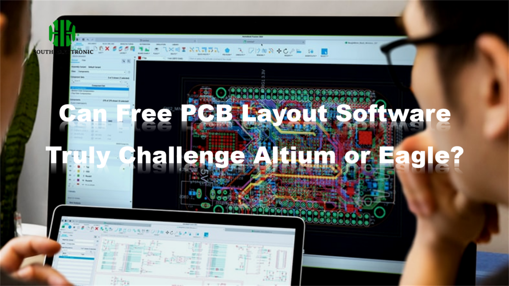
Free PCB design software helps beginners start affordably but struggles with complex projects. Learn key limitations & smart workarounds to leverage free tools effectively for prototypes & simple boards.
Can a standard FDM 3D printer make functional PCBs?
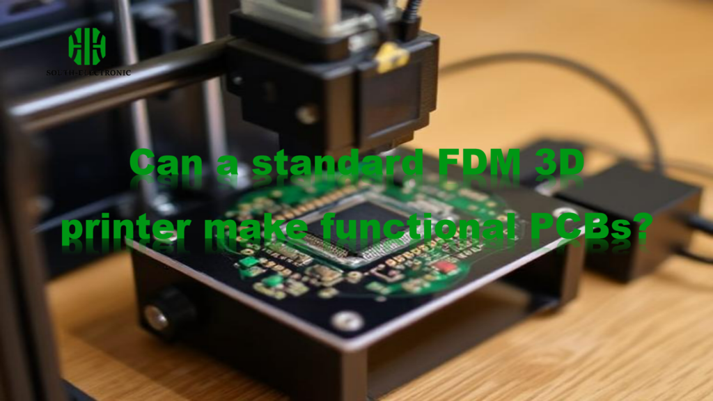
FDM printing creates quick DIY PCBs with conductive filament, ideal for low-power prototypes despite trace/soldering limits. Explore methods for faster, cheaper iterations.
Find the golden rule in Layout!

Top 10 PCB design rules for optimal layout and manufacturing: grid selection, routing, power planes, component grouping, panelization, DRC, silkscreen, capacitors. Boost reliability and cut costs.
