
What is the PCB Assembly Process?
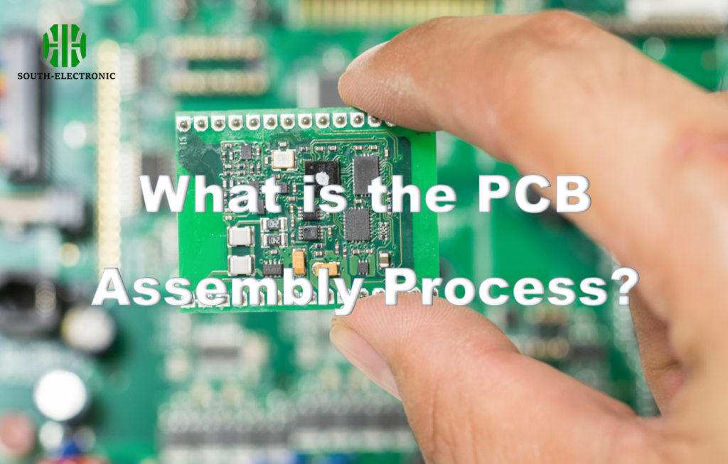
Discover key PCB assembly standards (ISO, IPC), realistic cost breakdowns, and timelines. Master manufacturing to avoid defects, budget surprises, and shipping delays for reliable electronics.
Do you need circuit boards in 48 hours?
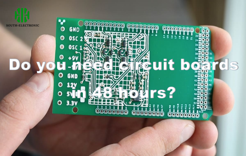
Get PCBs in 48 hours for emergencies but costs 2-3x more & has risks. Learn cost drivers, hidden pitfalls, and complexity limits.
What is a PCB laminate?
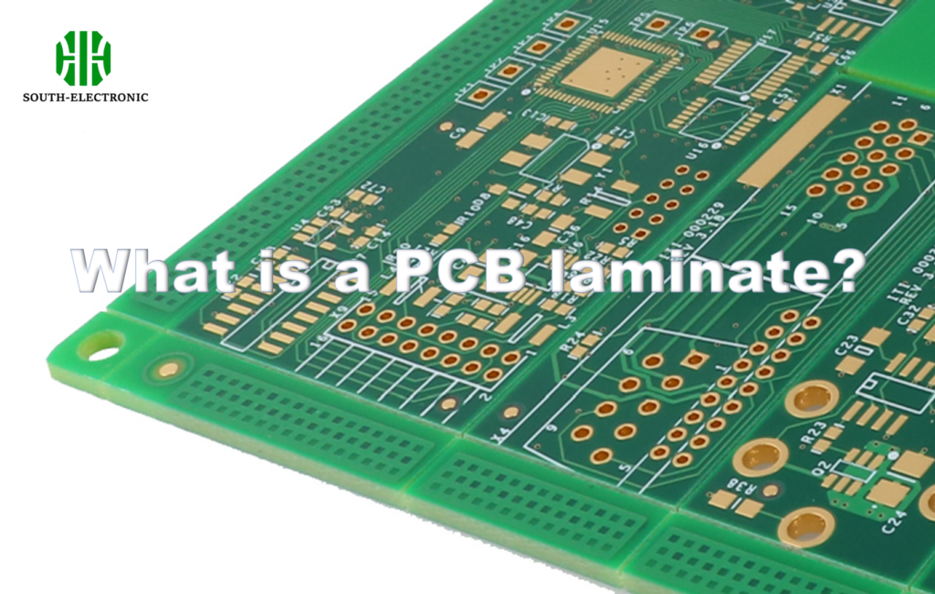
Master PCB laminate properties, defects, and material differences (prepreg vs core). Prevent high-speed signal issues, delamination, and costly failures. Essential for reliable circuit boards.
What Are Standard PCB Panel Sizes?

Optimize PCB costs and assembly: use standard panel sizes (e.g., 18″x24″), choose V-Score/Breakaway Tabs wisely, control costs via material utilization, and boost SMT efficiency with fiducials/thermal balance.
What is PCB backdrilling?
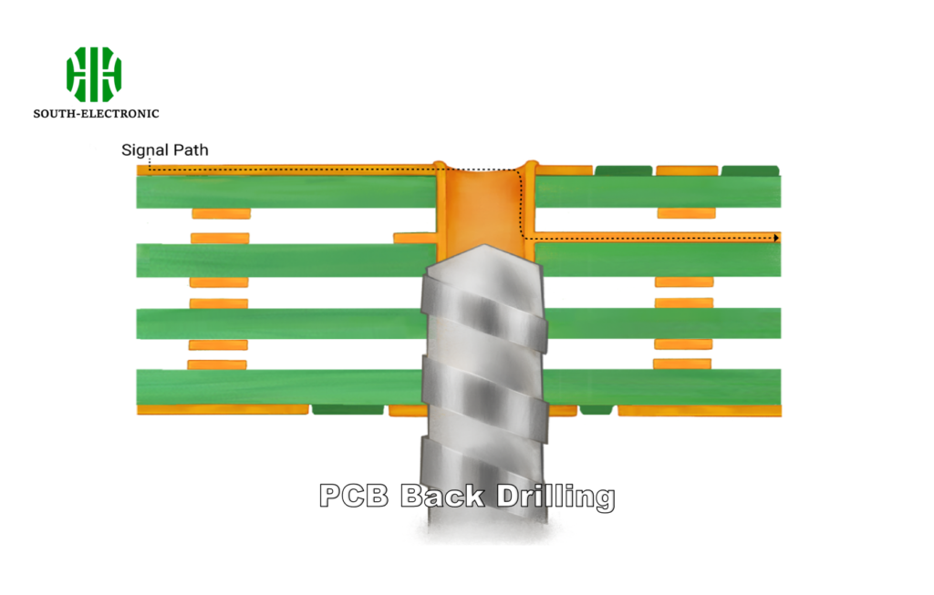
Learn how PCB backdrilling eliminates signal stubs for high-speed designs. Optimize layer stackups, apply the 3W rule to avoid crosstalk, and control costs by managing hole density, aspect ratio, materials, and tolerances.
How do you fix “invisible” PCB faults?
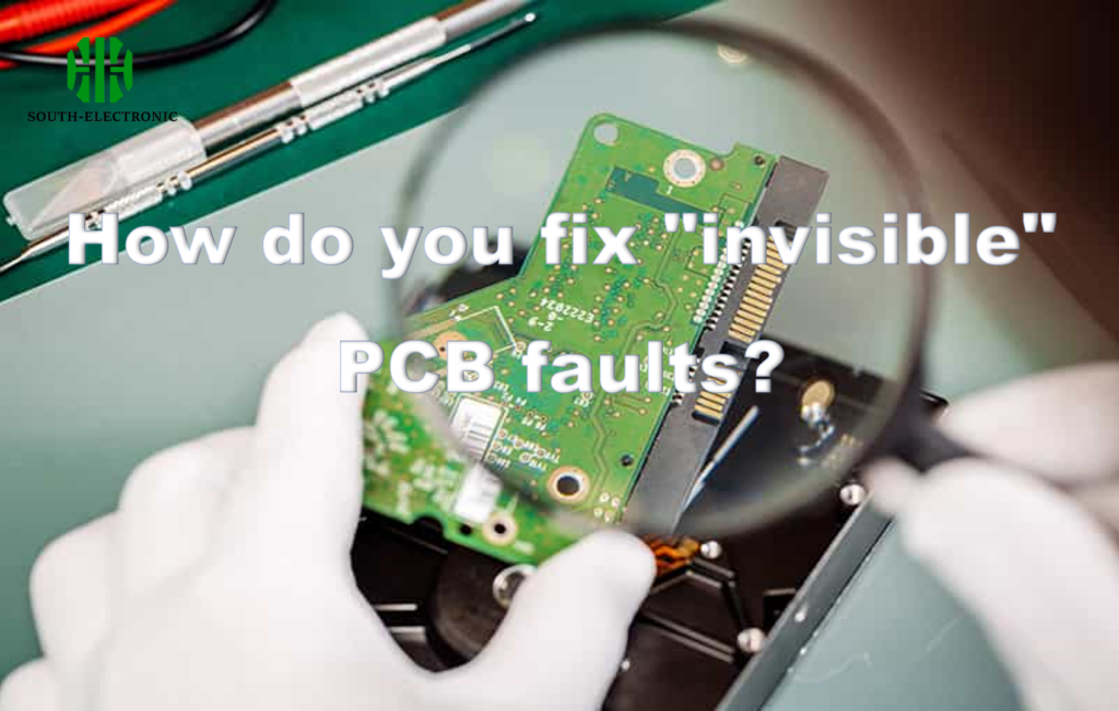
Diagnose hidden PCB failures caused by moisture/thermal stress. Learn cost breakdowns ($50-$800) and step-by-step trace repair techniques using expert-level inspection methods.
What are the Most Common Circuit Board Components?
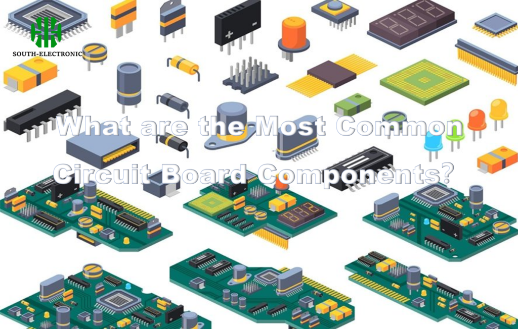
Master circuit board components: identify resistors, capacitors, transistors. Learn active vs passive, SMD vs through-hole differences, and crucial specs to build or repair electronics.
How do you choose between shield cans and conformal coatings?
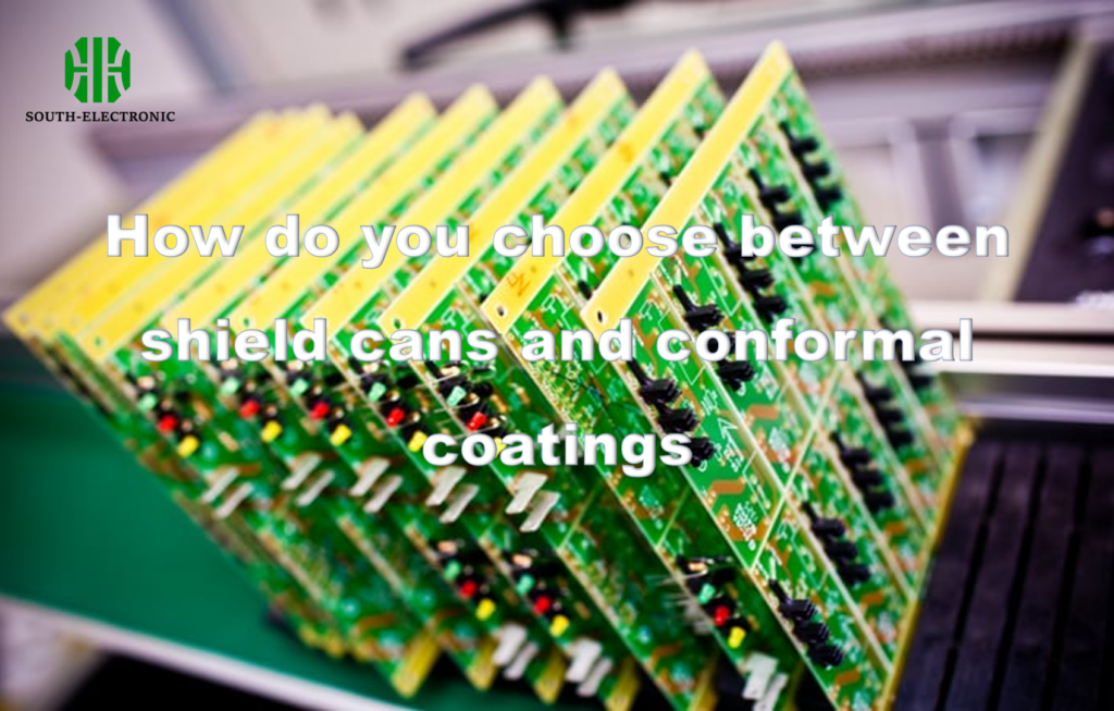
Optimize PCB shielding: Use cans for repairable EMI/impact protection and coatings for lightweight environmental sealing. Master grounding, flexible materials, and gasket cost-benefit.
What is HDI PCB and its Function?
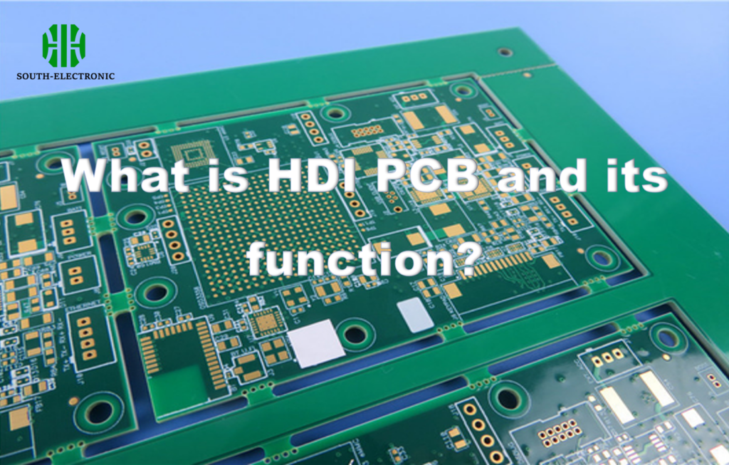
HDI PCBs use microvias for compact, high-performance electronics in smartphones, medical devices, and cars. Ultra HDI enables nano-scale circuits for aerospace/neural tech via submicro-vias and materials.
Why do microwave PCBs fail?
Microwave stopped working? PCB failures explained: overheating, design flaws, aging. Learn repairable vs hopeless cases & smart stackup choices to prevent future breakdowns.
